· AtlasPCB Engineering · Engineering · 11 min read
PCB Laser Drilling: Microvia Technology, Parameters, and Quality Control
Comprehensive guide to PCB laser drilling technology covering CO2 vs UV laser systems, microvia formation processes, aspect ratio limits, desmear requirements, quality inspection methods, and comparison with mechanical drilling.
PCB Laser Drilling: Microvia Technology, Parameters, and Quality Control
Laser drilling is the enabling technology behind HDI (High-Density Interconnect) PCBs. Without it, the microvias that make modern smartphones, wearables, automotive electronics, and high-performance computing possible simply wouldn’t exist. Understanding laser drilling — the physics, the process parameters, the quality requirements — is essential for any engineer designing boards that push beyond conventional mechanical drilling limits.
This article covers the full landscape of PCB laser drilling: the two primary laser types (CO2 and UV), the microvia formation process, critical process parameters, desmear requirements, quality inspection methods, and a detailed comparison with mechanical drilling.
The Role of Laser Drilling in HDI PCBs
A microvia, as defined by IPC-2226, is a blind via with a hole diameter of 150 µm (6 mil) or less. These tiny interconnects are the foundation of [HDI PCB technology]/blog/hdi-pcb-technology/), enabling:
- BGA escape routing under fine-pitch components (0.4 mm, 0.5 mm, 0.65 mm pitch)
- Layer transitions in sequential build-up (SBU) structures
- Stacked and staggered microvia architectures for high-layer-count HDI
- Via-in-pad designs that eliminate dog-bone routing
- Impedance-controlled short-stub vias that improve signal integrity
Mechanical drills cannot reliably produce holes below about 150 µm (6 mil) diameter. Below this threshold, laser drilling takes over. Modern HDI production relies on laser drilling for all build-up layer interconnections, and advanced designs may have more laser-drilled holes than mechanically drilled ones.
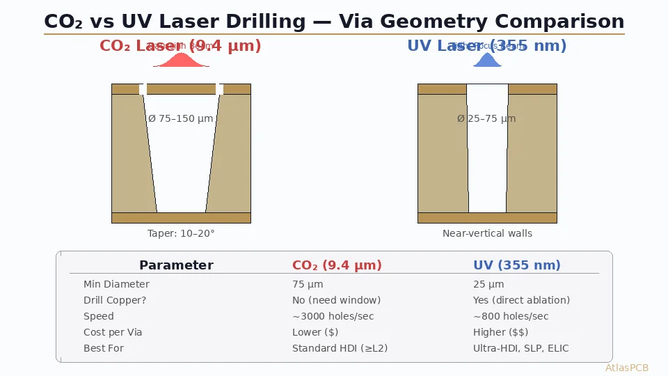
CO2 Laser Drilling
How It Works
CO2 lasers emit infrared light at a wavelength of 9.4 µm (or 10.6 µm, depending on the gas mixture). At this wavelength, the laser energy is efficiently absorbed by organic materials (epoxy resin, polyimide) but reflected by copper. This fundamental property defines the CO2 laser drilling process:
- Copper window opening: The copper on the entry layer must be pre-etched to create an opening (window) where the via will be drilled. This is done during the outer-layer photolithography step.
- Laser ablation: The CO2 laser fires through the copper window and ablates the dielectric material (resin + glass fiber) layer by layer.
- Target pad exposure: The laser stops at the copper target pad on the inner layer. Because copper reflects the CO2 wavelength, the target pad acts as a natural stop layer.
An alternative approach is conformal mask drilling: a thin layer of resin (or a special UV-absorbing mask) covers the copper, and the CO2 laser ablates this layer before drilling through the dielectric. This avoids the need for copper pre-etching but adds a process step.
CO2 Laser Parameters
| Parameter | Typical Range | Notes |
|---|---|---|
| Wavelength | 9.4 µm or 10.6 µm | Infrared |
| Pulse energy | 0.5–5 mJ | Adjusted for dielectric thickness |
| Pulse width | 5–25 µs | Shorter = less thermal damage |
| Pulse count | 1–5 pulses per hole | More pulses for thicker dielectrics |
| Beam diameter | 75–300 µm | Defines minimum via size |
| Drilling speed | 500–3,000 holes/second | Per beam; multi-beam systems exist |
| Minimum via diameter | 75 µm (3 mil) | Practical limit for production |
Advantages of CO2 Laser Drilling
- High throughput: Thousands of holes per second, making it cost-effective for high-volume production
- Proven technology: Decades of production history with well-understood process windows
- Natural copper stop: The target pad automatically stops the laser, reducing risk of damage to lower layers
- Lower capital and operating cost: Compared to UV systems
- Good for standard microvias: 75–150 µm diameter range covers most HDI designs
Limitations of CO2 Laser Drilling
- Cannot directly drill copper: Requires pre-etched window or conformal mask
- Minimum diameter ~75 µm: The long wavelength limits beam focus
- Thermal damage: Infrared energy heats surrounding material, creating a heat-affected zone (HAZ) of 10–25 µm
- Glass fiber residue: CO2 lasers do not ablate glass fibers as cleanly as resin; fiber stubs can protrude into the via
- Taper: CO2 drilled vias have a conical profile (top wider, bottom narrower); taper is typically 10–20%
UV Laser Drilling
How It Works
UV lasers (typically frequency-tripled Nd:YAG at 355 nm, or excimer lasers at 248 nm) operate at a wavelength that is absorbed by both dielectric materials and copper. This key difference from CO2 lasers enables direct copper ablation — the laser can drill through the copper entry layer without a pre-etched window.
The UV drilling process:
- Direct ablation: The UV laser fires directly on the copper surface. Each pulse removes a few micrometers of copper, then transitions to dielectric ablation.
- Precision shaping: The short wavelength allows tighter beam focus, enabling holes as small as 25 µm (1 mil).
- Clean sidewalls: The UV photochemical ablation process produces less thermal damage than CO2, resulting in cleaner hole walls.
UV Laser Parameters
| Parameter | Typical Range | Notes |
|---|---|---|
| Wavelength | 355 nm (Nd:YAG) or 248 nm (Excimer) | Ultraviolet |
| Pulse energy | 0.01–0.5 mJ | Much lower than CO2 |
| Pulse width | 10–50 ns | Nanosecond regime |
| Pulse count | 50–500+ pulses per hole | Many more pulses needed |
| Beam diameter | 15–75 µm | Enables ultra-fine vias |
| Drilling speed | 100–500 holes/second | Significantly slower than CO2 |
| Minimum via diameter | 25 µm (1 mil) | Production capability |
Advantages of UV Laser Drilling
- Direct copper ablation: No pre-etched window needed; simplifies the process
- Smaller holes: Down to 25 µm for advanced packaging and ultra-HDI
- Cleaner process: Photochemical ablation produces less thermal damage and less resin smear
- Better hole geometry: More cylindrical walls with less taper (5–10%)
- Glass fiber ablation: UV wavelength effectively ablates glass fibers, leaving cleaner sidewalls
Limitations of UV Laser Drilling
- Slow: 3–10× slower than CO2 for the same hole count
- Higher cost: Both capital equipment and operating (optics, gas) costs are higher
- Copper ablation is slow: Drilling through copper requires many pulses; thicker copper takes proportionally longer
- Smaller process window: Tighter parameter control required
The Microvia Formation Process
Regardless of laser type, the full microvia formation process involves multiple steps. Here is the complete sequence for a typical single-layer [blind microvia in an HDI build-up]/blog/hdi-pcb-stackup-design-advanced/):
Step 1: Lamination of Build-Up Layer
A prepreg/copper foil sheet is laminated onto the previously patterned core or sub-assembly. The build-up dielectric is typically 40–100 µm thick resin-coated copper (RCC) or prepreg.
Step 2: Copper Window Opening (CO2 Only)
For CO2 drilling, the copper foil on the entry side is photolithographically patterned to open windows where microvias will be drilled. Window diameter is typically 50–75 µm larger than the target via diameter to provide alignment margin.
Step 3: Laser Drilling
The panel is loaded into the laser drill machine. An automated vision system aligns the panel using fiducial marks. The laser then drills all microvias on the panel — potentially tens of thousands of holes.
Critical process control points:
- Beam energy calibration (verified before each panel)
- Focus height (distance from laser lens to panel surface)
- Panel flatness (warped panels cause defocusing)
- Pulse count optimization (enough to reach target pad, not so many as to damage it)
Step 4: Desmear
After laser drilling, the via bottoms have a thin layer of charred resin residue (smear) covering the target pad copper. This smear must be completely removed before plating.
Desmear methods:
Plasma Desmear (Dry Process)
- Gas mixture: CF₄/O₂ or CF₄/N₂
- Process: RF-excited plasma attacks organic residue
- Advantages: Uniform, no wet chemistry, environmentally cleaner
- Limitations: Slower, higher capital cost
Chemical Desmear (Wet Process)
- Three-step process: Swell → Etch → Neutralize
- Swell: Organic solvent swells the resin to open its structure
- Permanganate etch: Hot KMnO₄ solution (55–85 g/L, 75–85°C) oxidizes and removes smeared resin
- Neutralize: Acid reduction bath (HCl + H₂O₂ or proprietary) removes MnO₂ residue
- Advantages: High throughput, lower capital cost, well-established
- Limitations: Chemical waste management, potential for over-etch
Quality after desmear: The target pad should show clean, bright copper with no visible residue under 200× magnification. A shadow or discoloration indicates incomplete desmear.
Step 5: Electroless Copper Seeding
After desmear, the via walls are bare dielectric — they cannot be electroplated directly because they are non-conductive. An electroless copper deposition step deposits a thin (0.3–0.8 µm) conductive copper seed layer on all exposed surfaces, including the via walls and bottom.
Process: Catalyst activation (Pd/Sn colloid) → electroless copper bath (CuSO₄ + formaldehyde + NaOH + additives, 30–35°C)
Step 6: Electrolytic Copper Plating
With the seed layer in place, standard electrolytic plating fills the microvia with copper. For via-in-pad applications, copper-filled plating (also called via-fill plating) is used to completely fill the via cavity with copper, creating a flat, solderable surface.
Via-fill plating chemistry uses specialized organic additives:
- Suppressor: Adsorbs on flat surfaces to slow plating there
- Accelerator: Concentrates in concave areas (via cavity) to speed plating
- Leveler: Fine-tunes the fill profile for flat finish
The result is a via filled from bottom to top, with a slight dimple (≤15 µm) or protrusion on the surface. After planarization (surface grinding or chemical etch-back), the via-in-pad is ready for component mounting.
For more details on fill plating, see our article on [blind via fill technology]/blog/pcb-blind-via-fill-technology/).
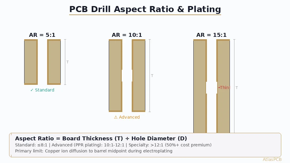
Microvia Aspect Ratio Limits
The aspect ratio of a microvia determines plating quality and reliability:
| Aspect Ratio | Plating Quality | Reliability | Application |
|---|---|---|---|
| ≤0.6:1 | Excellent fill | Highest reliability | Standard HDI |
| 0.6:1 – 0.8:1 | Good fill | High reliability | Standard HDI |
| 0.8:1 – 1.0:1 | Acceptable fill | Good reliability | Advanced HDI |
| 1.0:1 – 1.2:1 | Challenging fill | Moderate reliability | High-end HDI |
| >1.2:1 | Difficult, risk of voids | Lower reliability | Specialty only |
IPC-2226 recommendation: Maximum aspect ratio 1:1 for standard microvia processes. Anything beyond 1:1 requires qualification testing per IPC-6012.
Real-world target: Most fabricators target 0.8:1 as the sweet spot for reliable production. For a 75 µm deep dielectric, this means a minimum 94 µm (≈100 µm) via diameter.
Laser Drilling vs. Mechanical Drilling: Comprehensive Comparison
| Feature | CO2 Laser | UV Laser | Mechanical CNC |
|---|---|---|---|
| Minimum hole size | 75 µm (3 mil) | 25 µm (1 mil) | 150 µm (6 mil) |
| Maximum hole size | 300 µm (12 mil) | 150 µm (6 mil) | 6.35 mm (250 mil) |
| Hole depth | Single dielectric layer (40–100 µm) | Single dielectric layer | Full board thickness |
| Speed | 500–3,000 holes/sec | 100–500 holes/sec | 1–5 holes/sec |
| Hole shape | Conical (10–20% taper) | Near-cylindrical (5–10% taper) | Cylindrical |
| Copper drilling | No (needs window) | Yes (direct) | Yes (mechanical) |
| Positioning accuracy | ±15–25 µm | ±10–20 µm | ±25–50 µm |
| Heat-affected zone | 10–25 µm | 3–10 µm | Minimal thermal, but mechanical stress |
| Tooling wear | No physical tool wear | No physical tool wear | Drill bit wears after 2,000–5,000 hits |
| Capital cost | Medium | High | Low–Medium |
| Via types | Blind only | Blind only | Through, blind (controlled-depth), buried |
Quality Inspection for Laser-Drilled Microvias
Visual Inspection (Automated Optical Inspection — AOI)
Post-drilling AOI checks:
- Via position relative to pads (registration)
- Via diameter consistency
- Missing vias (laser misfire or blocked beam)
- Oversized vias (excessive energy)
Cross-Section Analysis
The definitive quality check. Microsection examination reveals:
- Via profile: Shape (cylindrical vs. conical), taper angle, bottom diameter
- Desmear quality: Clean target pad vs. residual smear
- Copper plating: Thickness uniformity, fill completeness, dimple depth
- Interface quality: Bond between electroless copper and dielectric; bond between plating and target pad
- Glass fiber stubs: Protrusions from incomplete fiber ablation (CO2 issue)
Electrical Testing
- Resistance measurement: Via chain (daisy chain) resistance should be consistent across the panel
- Insulation resistance: Between adjacent vias; confirms no copper bridging or conductive debris
- High-potential (HiPot) testing: Confirms dielectric integrity around the via
Thermal Reliability Testing
Per IPC-TM-650 Method 2.6.27 (Thermal Shock and Continuity — Microvia), microvias are subjected to thermal cycling and resistance monitoring. Failure criteria:
- Resistance increase >10%: Connection degradation
- Open circuit: Complete via failure
- Delamination: Separation of plating from dielectric or target pad (visible in post-test cross-section)
IPC-6012 Class 3 requires that microvias survive a specified number of thermal cycles (typically 100–300 cycles, –55°C to +125°C, or IST equivalent) without exceeding the resistance failure threshold.
Common Laser Drilling Defects and Root Causes
| Defect | Root Cause | Prevention |
|---|---|---|
| Incomplete drilling (resin at bottom) | Insufficient pulse energy or count | Optimize pulse recipe per dielectric thickness |
| Target pad damage (cratering) | Excessive energy on copper | Reduce pulse count; improve process window |
| Oversized via | Energy too high; beam out of focus | Calibrate energy; verify focus height |
| Undersized via | Energy too low; beam degradation | Maintain optics; calibrate regularly |
| Misregistration | Panel alignment error; thermal expansion | Improve fiducial recognition; temperature control |
| Glass fiber stubs | CO2 laser limitation | Add UV cleanup pass; extend desmear |
| Excessive taper | Multiple high-energy pulses | Use more, lower-energy pulses |
| Copper splash | Exploded copper debris from window edge | Improve window etch process; use conformal mask |
Future Trends in Laser Drilling
The evolution of laser drilling technology continues to push boundaries:
- Hybrid CO2/UV systems: Machines with both laser sources, automatically selecting the optimal laser for each hole type
- Multi-beam systems: Splitting a single laser into multiple beams for parallel drilling, multiplying throughput
- Ultra-short pulse (femtosecond) lasers: Virtually zero thermal damage; enables drilling of exotic materials (glass, ceramic)
- Larger panel formats: Moving from 510 mm × 610 mm to 600 mm × 720 mm and larger panels to improve material utilization
- Automated via quality inspection: Inline camera systems that inspect every via immediately after drilling
Summary
Laser drilling is the gateway technology for HDI PCB manufacturing. The key takeaways:
- CO2 lasers are the production workhorse for microvias ≥75 µm — fast, reliable, cost-effective
- UV lasers enable ultra-fine vias down to 25 µm with superior hole quality — essential for advanced packaging
- Desmear is non-negotiable — incomplete desmear is the #1 root cause of microvia reliability failures
- Aspect ratio ≤1:1 for reliable copper fill plating; target 0.8:1 for production robustness
- Quality control requires cross-section analysis, electrical testing, and thermal reliability validation
- Choose the right laser for your design requirements — and work with a fabricator who has both options
Whether your design needs standard HDI microvias or cutting-edge ultra-fine via structures, understanding the laser drilling process helps you make informed decisions about via sizing, stackup design, and fabricator selection.
Ready to start your project? Upload your Gerbers for a free engineering review, or talk to an engineer about your design requirements.
Further Reading
- [PCB Copper Plating Process: Electroless vs Electrolytic Copper for HDI Vias and High-Density Interconnects]/blog/pcb-copper-plating-electroless-vs-electrolytic-hdi-vias/)
- [Buried Via Technology in High-Density PCBs: Design Rules, Fabrication & Cost]/blog/pcb-buried-via-technology/)
- [Rogers PCB Fabrication: Material Sourcing, Lead Times & Quality Control]/blog/rogers-pcb-fabrication/)
- [HDI PCB Design for 5G Antenna Integration: Signal Integrity Challenges in Millimeter-Wave Applications]/blog/hdi-5g-antenna-integration-pcb-design/)
- [PCB Via Size Guide: Mechanical, Laser & Microvia Dimensions]/blog/pcb-via-size-selection-guide/)
- Our Manufacturing Capabilities
About AtlasPCB — We specialize in complex PCB manufacturing for HDI, RF, and high-reliability applications. Explore our HDI PCB manufacturing capabilities . Every order includes free engineering review. Get your quote.
Reviewed by AtlasPCB Engineering Team — IPC-certified manufacturing specialists with 15+ years of production experience in HDI, RF, and high-reliability PCB fabrication. Content based on factory floor data and real customer design reviews.
- laser-drilling
- microvia
- hdi
- pcb-manufacturing
- quality-control