· AtlasPCB Engineering · Engineering · 12 min read
PCB Blind Via Fill Technology: Copper Plating, Epoxy Fill & IPC-4761 Type VII Explained
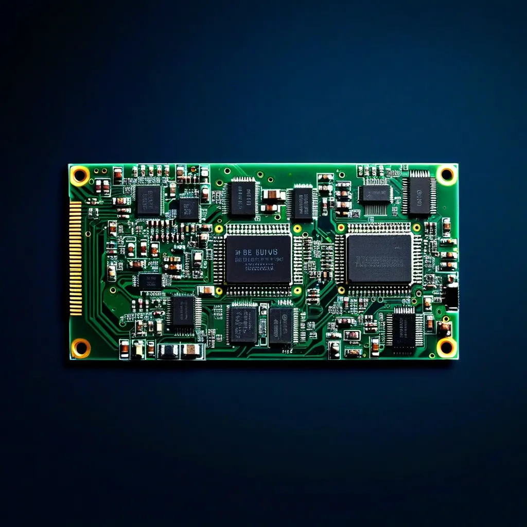
Complete engineering guide to blind via filling methods including electrolytic copper fill, conductive epoxy, and non-conductive epoxy. Covers IPC-4761 Type VII requirements, void-free fill criteria, dimple specifications, and via-in-pad design rules for HDI and BGA applications.
PCB Blind Via Fill Technology: Complete Engineering Guide
Blind via filling has become one of the most critical process capabilities in modern PCB manufacturing. As component packages shrink and pin densities increase—particularly with 0.4mm and 0.5mm pitch BGAs—the ability to place vias directly under component pads demands blind vias that are completely filled, planarized, and electrically reliable. This guide covers the engineering fundamentals of blind via fill technology, from process chemistry to acceptance criteria per [IPC standards and manufacturing specifications]/blog/pcb-manufacturing-process/).
Why Blind Via Filling Matters
Traditional blind vias leave an open cavity after drilling and plating. This creates several problems in high-density designs:
Solder wicking during assembly: Open blind vias beneath BGA pads act as capillaries, drawing molten solder away from the joint during reflow. A 0.2mm diameter unfilled blind via can absorb 0.008mm³ of solder—enough to cause insufficient solder volume on 0.4mm pitch BGA balls, resulting in open joints or head-in-pillow defects.
Outgassing during reflow: Trapped moisture and volatile residues in unfilled via cavities expand during lead-free reflow temperatures (peak 245-260°C), creating blow holes in solder joints. This is particularly problematic in double-sided reflow processes where the second reflow cycle can force contaminants through previously sealed joints.
Reduced thermal conductivity: Unfilled vias provide only a thin copper barrel (typically 20-25μm) for thermal conduction. For power management ICs with thermal pads, this limits heat transfer from the component to internal ground planes by 60-80% compared to solid copper-filled vias.
Planarization requirements for stacking: In [HDI designs with stacked microvias]/blog/hdi-pcb-technology/), the via surface must be flat enough to serve as a reliable landing pad for the next via layer. Surface irregularities greater than 15μm can cause misregistration, insufficient copper connection, or void formation in the stacked via.
IPC-4761 Via Protection Classification
IPC-4761, “Design Guide for Protection of Printed Board Via Structures,” defines seven types of via protection. For blind via filling, three types are most relevant:
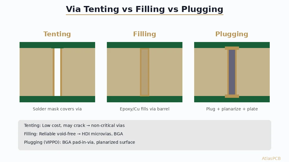
Type V — Filled (Non-Conductive)
The via is filled with non-conductive material (typically epoxy-based paste) that is cured and planarized. No metal cap is applied. This type is suitable for preventing solder wicking but does not provide additional electrical or thermal conductivity through the via fill material.
Key specifications:
- Fill material: Non-conductive epoxy paste (CTE matched to copper: 15-20 ppm/°C)
- Cure temperature: 150-180°C for 45-90 minutes
- Tg of fill material: >150°C (must survive lead-free reflow)
- Planarization: Diamond-grit belt or ceramic cup wheel
Type VI — Filled and Capped (Non-Conductive Fill + Metal Cap)
The via is filled with non-conductive material, planarized, and then over-plated with copper to create a continuous metal surface. This is the most common approach for [via-in-pad designs with BGA packages]/blog/pcb-pad-design-bga-qfn/).
Key specifications:
- Fill material: Same as Type V
- Cap plating: 15-25μm electrolytic copper over the planarized fill
- Adhesion: Cap must withstand 5× solder float at 288°C per IPC-TM-650 2.4.13
- Surface dimple after cap plating: ≤15μm (typically ≤10μm achievable)
Type VII — Filled and Capped (Conductive Fill + Metal Cap)
The via is filled with conductive material—either electrolytic copper or conductive epoxy—and capped with copper. This provides the best electrical and thermal performance and is required for high-reliability applications per IPC-6012 Class 3/A.
Key specifications:
- Fill material: Electrolytic copper (preferred) or silver-filled conductive epoxy
- Electrical conductivity of fill: ≥90% IACS for copper fill; 0.001-0.01 Ω·cm for conductive epoxy
- Thermal conductivity: 390 W/m·K (copper fill) vs. 3-15 W/m·K (conductive epoxy)
- Cap plating: 15-25μm electrolytic copper
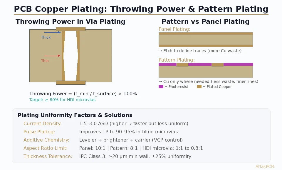
Electrolytic Copper Fill Process
Electrolytic copper filling is the gold standard for blind via fill. The process uses specialized plating chemistry with differential inhibition to preferentially deposit copper at the bottom of the via while suppressing plating at the opening (the “bottom-up” fill mechanism).
Chemistry Components
The copper fill plating bath consists of:
- Copper sulfate (CuSO₄·5H₂O): 200-250 g/L — provides copper ions
- Sulfuric acid (H₂SO₄): 50-80 g/L — enhances conductivity and throwing power
- Chloride ions (Cl⁻): 40-70 ppm — essential for additive synergy
- Suppressor (PEG-based polymer): 2-8 mL/L — adsorbs preferentially at high-current-density areas (via opening) to inhibit plating
- Accelerator (SPS/MPS): 2-8 mL/L — concentrates at low-current-density areas (via bottom) to enhance plating
- Leveler (nitrogen-containing dye): 0.5-3 mL/L — provides additional differential plating control
Process Parameters
| Parameter | DC Plating | Pulse/Pulse-Reverse |
|---|---|---|
| Current density | 1.5-3.0 ASF (16-32 A/m²) | 2.0-4.0 ASF (22-43 A/m²) |
| Plating time | 90-180 min | 60-120 min |
| Temperature | 22-28°C | 22-28°C |
| Agitation | Air + cathode movement | Air + cathode movement |
| Anode type | Phosphorized Cu (0.04-0.06% P) | Insoluble (IrO₂/Ti) |
| Filtration | Continuous, 1-5μm | Continuous, 1-5μm |
Pulse-reverse parameters (typical):
- Forward pulse: 10-20 ms at 3-4 ASF
- Reverse pulse: 1-3 ms at 5-10 ASF
- Duty cycle: 75-90% forward
Pulse-reverse plating offers significant advantages for blind via fill. The reverse pulse dissolves preferentially from the via opening (where copper is thickest), maintaining the bottom-up fill profile. This enables faster fill times and better void-free performance, particularly for high aspect ratio blind vias (depth:diameter > 0.8:1).
Aspect Ratio Considerations
The fill-ability of blind vias is fundamentally limited by the aspect ratio and absolute geometry:
| Via Diameter | Via Depth | Aspect Ratio | Fill Difficulty |
|---|---|---|---|
| 150μm | 65μm | 0.43:1 | Standard |
| 100μm | 65μm | 0.65:1 | Moderate |
| 100μm | 100μm | 1.0:1 | Challenging |
| 75μm | 65μm | 0.87:1 | Challenging |
| 75μm | 100μm | 1.33:1 | Very difficult |
| 50μm | 50μm | 1.0:1 | Advanced |
For aspect ratios above 1.0:1, specialized chemistry and precise process control are essential to prevent “pinch-off” (premature closure at the via mouth that traps a void inside).
Non-Conductive Epoxy Fill Process
For applications where the full thermal/electrical performance of copper fill is not required, non-conductive epoxy fill provides a cost-effective alternative. This process is widely used for Type V and Type VI via protection.
Process Steps
Via preparation: Blind vias are plated with a standard copper barrel (20-25μm minimum per IPC-6012 Class 3). Surfaces are cleaned and micro-etched for adhesion.
Paste application: Screen printing or vacuum-assisted dispensing forces epoxy paste into the blind vias. Vacuum application (50-100 mbar) improves fill completeness by removing trapped air.
Initial cure: Partial cure at 120-130°C for 20-30 minutes to solidify the epoxy enough for handling.
Planarization: Belt grinding with 600-1200 grit ceramic media removes excess epoxy, creating a flush surface with the copper foil. Target: ±5μm of surrounding copper surface.
Final cure: Full cure at 150-180°C for 45-90 minutes. The fill material must achieve full cross-linking to withstand reflow temperatures.
Cap plating (Type VI only): Standard electrolytic copper plating (20-25μm) over the entire surface, followed by circuit imaging and etching.
Epoxy Fill Material Properties
| Property | Requirement | Typical Value |
|---|---|---|
| Tg (DSC) | >150°C | 155-175°C |
| CTE (below Tg) | <30 ppm/°C | 18-25 ppm/°C |
| CTE (above Tg) | <80 ppm/°C | 50-70 ppm/°C |
| Moisture absorption | <0.5% | 0.2-0.3% |
| Shrinkage | <2% | 0.5-1.5% |
| Adhesion to copper | >0.8 N/mm | 1.0-1.5 N/mm |
| Thermal conductivity | — | 0.5-3.0 W/m·K |
The CTE mismatch between epoxy fill (18-25 ppm/°C) and copper barrel (17 ppm/°C) must be minimized to prevent delamination during thermal cycling. IPC-6012 Class 3 requires no separation after 100 cycles of -55°C to +125°C per IPC-TM-650 2.6.7.2.
Conductive Epoxy Fill
Conductive epoxy fills occupy a middle ground between non-conductive epoxy and solid copper. These materials consist of a polymer matrix loaded with silver or copper particles.
Properties Comparison
| Property | Non-Conductive Epoxy | Conductive Epoxy | Electrolytic Copper |
|---|---|---|---|
| Electrical resistivity | >10¹⁰ Ω·cm | 0.001-0.01 Ω·cm | 1.7×10⁻⁶ Ω·cm |
| Thermal conductivity | 0.5-3 W/m·K | 3-15 W/m·K | 390 W/m·K |
| CTE | 18-25 ppm/°C | 20-35 ppm/°C | 17 ppm/°C |
| Cost (relative) | 1× | 2-3× | 3-5× |
| Reliability | Good | Good | Excellent |
Conductive epoxy is primarily used in applications requiring moderate electrical continuity through the via fill but where the cost of full copper fill is not justified.
Void-Free Fill Criteria and Inspection
IPC-6012 Class 3 Requirements
IPC-6012, Rev. E, Section 3.6.2 specifies the following acceptance criteria for filled vias:
- Void area: Less than 25% of the via cross-sectional area in any single cross-section
- Maximum single void dimension: No void exceeding 50μm in any direction
- Dimple: Surface depression ≤15μm below the surrounding copper plane
- Cap integrity: No separation between cap plating and fill material
- Barrel plating: Minimum 20μm copper barrel thickness maintained
For automotive and aerospace applications requiring [IPC-6012 Class 3/A]/blog/pcb-via-reliability-testing/), the requirements are more stringent:
- Void area: Less than 10% in any cross-section
- Dimple: ≤10μm
- Additional thermal cycling qualification: 200 cycles per IST (Interconnect Stress Testing)
Inspection Methods
Cross-sectioning (destructive): The definitive method. Coupon sections are polished to the via center and examined at 100-500× magnification. Void area is measured using image analysis software. Per IPC-TM-650 Method 2.1.1, a minimum of 3 microsections per lot are required.
X-ray inspection (non-destructive): 2D X-ray can identify large voids (>30μm) and gross fill defects. For critical applications, computed tomography (CT) X-ray at 1-5μm resolution can generate 3D void maps without destroying the board.
Acoustic microscopy (C-SAM): Can detect delamination between fill material and copper barrel. Useful for process qualification but limited spatial resolution for small blind vias.
Via-in-Pad Design Rules for Blind Via Fill
When designing blind vias intended for filling and via-in-pad placement, several critical design rules must be followed:
Geometric Rules
Via diameter vs. pad diameter: The via must be at least 100μm smaller in diameter than the BGA pad. For 0.5mm pitch BGAs with 280μm pads, maximum via diameter is 180μm. For 0.4mm pitch with 220μm pads, maximum via diameter is 120μm.
Via centering: The via must be centered within the pad with ≤25μm offset. Misregistration beyond this can cause asymmetric solder joint formation and reliability issues.
Annular ring on target pad: Minimum 50μm annular ring between via edge and pad edge per IPC-2226 Level A (standard HDI).
Via depth-to-diameter ratio: Keep below 1:1 for standard processes, below 0.8:1 for maximum reliability. Deeper aspect ratios require [advanced HDI stackup design]/blog/hdi-pcb-stackup-design-advanced/) and specialized fill chemistry.
Thermal Design Considerations
For thermal pad applications (power ICs, LED substrates), the via array beneath the thermal pad must be designed to maximize heat transfer:
- Via pitch: 0.8-1.2mm center-to-center for copper-filled vias
- Via count: Calculate based on thermal resistance requirements. Each 0.3mm diameter copper-filled via through 1.6mm board provides approximately 0.05°C/W thermal resistance reduction
- Fill material selection: Copper fill (390 W/m·K) reduces thermal resistance by 100-200× compared to non-conductive epoxy fill (1-3 W/m·K)
Electrical Considerations
Filled blind vias in signal paths must be evaluated for their impact on [signal integrity]/blog/signal-integrity-pcb-design-guide/):
- Via inductance: Copper-filled blind vias exhibit 15-25% lower inductance than hollow plated vias due to the solid copper core reducing the magnetic field concentration
- Via capacitance: Slightly increased (5-10%) compared to hollow vias due to the higher effective dielectric constant of the copper-filled structure
- Via resistance: 0.5-2 mΩ for copper-filled 100μm diameter blind via through 65μm depth, versus 3-5 mΩ for barrel-plated only
Sequential Lamination Integration
Blind via filling is inherently integrated into the [sequential lamination process for HDI boards]/blog/multilayer-pcb-manufacturing-process-explained/). The typical process flow is:
Two-Stage Sequential Build (1+N+1)
- Fabricate core layers (inner layers of the N-layer core)
- Laminate core
- Drill through-holes in core
- Plate through-holes
- Image and etch core outer layers
- First sequential lamination: Add buildup layers (prepreg + copper foil) on both sides
- Laser drill blind vias: CO₂ or UV laser, 75-150μm diameter
- Desmear and seed: Plasma or permanganate desmear, electroless copper seed (0.5-1.0μm)
- Fill plate blind vias: Electrolytic copper fill process (90-180 minutes)
- Planarize: Belt grinding to achieve ≤15μm dimple
- Image and etch outer layers
- Solder mask, surface finish, routing
Three-Stage Sequential Build (2+N+2)
For designs requiring stacked microvias (common in mobile device and advanced networking applications), the filled blind via surface must be flat enough to serve as a reliable landing pad for the second-level via. Requirements become more stringent:
- Dimple after planarization: ≤10μm (not the standard 15μm)
- Surface roughness (Ra): <2μm to ensure proper copper adhesion for the next buildup layer
- Void tolerance: <10% area to prevent outgassing during subsequent lamination cycles
The stacked via configuration relies entirely on the quality of the first-level via fill. A void in the bottom via can propagate upward during the second lamination cycle, creating a reliability failure path that may not be detected until thermal cycling in the field.
Common Defects and Root Causes
Center Void (Keyhole)
Description: A void trapped in the center of the via, typically elongated vertically. The most common fill defect.
Root causes:
- Insufficient suppressor concentration → plating at opening too fast
- Current density too high → premature pinch-off
- Inadequate agitation → depleted copper ions at via bottom
- Aspect ratio too high for the chemistry capability
Countermeasures: Reduce current density to 1.5-2.0 ASF, increase suppressor concentration by 10-20%, implement pulse-reverse plating, verify agitation uniformity.
Edge Void
Description: Voids along the sidewall of the via, between the copper fill and the barrel plating.
Root causes:
- Inadequate desmear → poor adhesion between fill copper and barrel
- Contamination on barrel surface before fill plating
- Air bubble trapped during immersion
Countermeasures: Verify desmear process (permanganate etch-back 8-15μm per IPC-6012), implement pre-clean cycle before fill plating, ensure slow immersion with wetting agent.
Excessive Dimple
Description: Surface depression greater than 15μm after planarization and/or cap plating.
Root causes:
- Incomplete fill → insufficient plating time
- Fill material shrinkage (epoxy) → >2% volume loss during cure
- Aggressive planarization → over-grinding
Countermeasures: Extend plating time by 15-20%, switch to low-shrinkage fill material, calibrate planarization parameters with test panels.
Process Qualification and Reliability Testing
Before production release, blind via fill processes must be qualified through a comprehensive test program:
Microsection evaluation: 32 cross-sections minimum per IPC-6012, evaluating void area, dimple, barrel thickness, and fill completeness
Thermal shock: 6× solder float at 288°C for 10 seconds per IPC-TM-650 2.4.13 — no barrel cracking, delamination, or fill separation
IST (Interconnect Stress Testing): 500+ cycles to failure, with minimum requirement of 200 cycles per IPC-6012 Class 3/A
CAF testing (Conductive Anodic Filament): Per IPC-TM-650 2.6.25, verify no conductive filament growth between adjacent filled vias at 85°C/85% RH under 100V DC bias for 500 hours
Thermal cycling: -55°C to +125°C, 100 cycles minimum per IPC-TM-650 2.6.7.2, with resistance change <10%
Cost Considerations
Blind via filling adds significant cost to the PCB manufacturing process. Engineers should understand the cost drivers to make informed design decisions:
| Fill Method | Additional Cost vs. Unfilled | Typical Lead Time Impact |
|---|---|---|
| Non-conductive epoxy (Type V) | +15-25% | +1-2 days |
| Epoxy fill + cap plate (Type VI) | +25-40% | +2-3 days |
| Copper electroplating fill (Type VII) | +35-60% | +2-4 days |
Cost optimization strategies:
- Use Type VI (epoxy fill) where Type VII (copper fill) is not required by thermal or electrical specifications
- Minimize blind via count by optimizing [component placement and routing density]/blog/pcb-stackup-design-guide/)
- Standardize via diameters to reduce laser drill program complexity
- Group blind vias by depth to minimize sequential lamination cycles
Summary
Blind via fill technology is a cornerstone of modern HDI PCB manufacturing. Whether using electrolytic copper fill for maximum performance or non-conductive epoxy for cost efficiency, the process demands precise control of chemistry, plating parameters, and inspection protocols. Designing for manufacturability—maintaining aspect ratios below 1:1, specifying appropriate IPC-4761 fill types, and understanding the trade-offs between fill methods—is essential for achieving reliable, high-yield production.
Ready to start your project? Upload your Gerbers for a free engineering review, or talk to an engineer about your design requirements.
Further Reading
- [HDI PCB Design Guide: Stackup Rules, Via Structures & DFM Checklist]/blog/hdi-pcb-design-guide/)
- [PCB Sequential Lamination: Process, Design Rules, and When You Need It]/blog/pcb-sequential-lamination/)
- [How to Design an HDI Stackup: Step-by-Step for First-Time Designers]/blog/how-to-design-hdi-stackup/)
- [Via-in-Pad Design: Filled, Capped, and Plated Over — Complete Guide]/blog/via-in-pad-design/)
- [Blind Via vs Buried Via: Design Rules, Cost Impact & When to Use Each]/blog/blind-via-vs-buried-via/)
About AtlasPCB — We specialize in complex PCB manufacturing for HDI, RF, and high-reliability applications. Explore our HDI PCB manufacturing capabilities . Every order includes free engineering review. Get your quote.
Reviewed by AtlasPCB Engineering Team — IPC-certified manufacturing specialists with 15+ years of production experience in HDI, RF, and high-reliability PCB fabrication. Content based on factory floor data and real customer design reviews.
- blind-via
- via-filling
- hdi-pcb
- pcb-manufacturing