· AtlasPCB Engineering · Engineering · 8 min read
Differential Pair Routing Rules for 10+ Gbps SerDes: PCIe 5.0, USB4, and Beyond
Master differential pair routing for high-speed SerDes interfaces. Complete design rules for impedance control, length matching, via transitions, and reference plane management at 10-32 Gbps.

The Challenge of 10+ Gbps Differential Signaling
Modern SerDes interfaces push data rates that would have been considered impossible on organic PCB substrates just a decade ago. PCIe 5.0 at 32 GT/s, USB4 at 20 Gbps per lane, 100GBASE-KR4 at 25.78 Gbps NRZ, and the emerging 112G PAM4 interfaces for data center switches — all demand PCB routing precision that leaves zero margin for guesswork.
At these speeds, the PCB is not just a carrier. It is a transmission line system where every geometric discontinuity, every impedance variation, every fraction of a millimeter of length mismatch manifests as measurable signal degradation on an eye diagram. The difference between a working and a failing channel is often less than 1 dB of insertion loss margin.
This guide provides concrete, production-proven routing rules for modern high-speed differential pairs — the kind of practical knowledge that bridges the gap between simulation results and boards that pass compliance testing on the first spin.
Impedance Targets by Interface Standard
Each SerDes standard specifies its own impedance target. Getting this wrong means the board cannot pass channel compliance:
| Interface | Data Rate | Zdiff Target | Tolerance | Zse (single-ended) |
|---|---|---|---|---|
| PCIe 4.0 | 16 GT/s | 85 Ω | ±15% | 42.5 Ω |
| PCIe 5.0 | 32 GT/s | 85 Ω | ±7% | 42.5 Ω |
| PCIe 6.0 | 64 GT/s PAM4 | 85 Ω | ±5% | 42.5 Ω |
| USB4 Gen 3 | 20 Gbps | 85 Ω | ±10% | 42.5 Ω |
| 100G Ethernet KR4 | 25.78 Gbps | 100 Ω | ±10% | 50 Ω |
| 400G Ethernet KR8 | 53.125 Gbps PAM4 | 100 Ω | ±7% | 50 Ω |
| HDMI 2.1 | 12 Gbps | 100 Ω | ±10% | 50 Ω |
Note the trend: as data rates increase, impedance tolerance tightens. PCIe 5.0’s ±7% tolerance means your fabricator must hit 79.05-90.95 Ω — a 12 Ω window that requires controlled impedance manufacturing processes with per-panel verification.
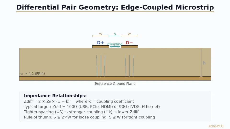
Trace Geometry and Stackup Design
Edge-Coupled Microstrip (Outer Layers)
For top/bottom layer routing — the most common geometry for connector breakout:
Key relationships:
- Width (W): Determined by impedance target and stackup. Typically 3.5–5 mil for 85 Ω on low-loss materials
- Gap (S): Usually 1-2× trace width. Tighter coupling (smaller S) reduces EMI but increases crosstalk sensitivity
- Height (H): Dielectric thickness to reference plane. Typically 3–5 mil for outer layers
Design tip: Keep the W/H ratio between 0.8 and 1.2 for optimal manufacturing control. Extremely narrow traces on thick dielectrics (low W/H) are difficult to etch consistently.
Edge-Coupled Stripline (Inner Layers)
Inner-layer routing between two reference planes — preferred for long parallel runs:
- More shielded from adjacent layer crosstalk
- Dual reference planes provide better return current paths
- Typically slightly narrower traces due to the “clamped” field pattern
- Requires careful lamination registration (trace-to-plane alignment)
For detailed stackup calculation methods, including worked examples with common low-loss materials, see our impedance design guide.
Material Impact on Geometry
The laminate’s dielectric constant (Dk) directly affects trace width:
- Standard FR-4 (Dk ≈ 4.2): Wider traces for same impedance
- Mid-loss (Megtron 4, Dk ≈ 3.7): Moderate trace width
- Ultra-low-loss (Megtron 7, Dk ≈ 3.4): Narrower traces
A 10% Dk reduction typically allows 5-8% narrower traces at the same impedance. This matters for routing density in BGA breakout fields where every mil counts.
Length Matching Rules
Intra-Pair Matching (P/N Skew)
The length difference between the positive and negative traces of a single differential pair:
| Data Rate | Max Intra-Pair Skew | Equivalent Time |
|---|---|---|
| 10 Gbps | 10 mil (0.25 mm) | 1.4 ps |
| 16 Gbps (PCIe 4.0) | 7 mil (0.18 mm) | 1.0 ps |
| 25 Gbps (100GbE) | 5 mil (0.13 mm) | 0.7 ps |
| 32 Gbps (PCIe 5.0) | 5 mil (0.13 mm) | 0.7 ps |
| 56 Gbps (PAM4) | 3 mil (0.08 mm) | 0.4 ps |
Compensation rules:
- Apply serpentine compensation immediately where the skew is introduced (via pad asymmetry, connector pin escape)
- Never accumulate multiple skew sources and compensate at the end
- Serpentine amplitude should be ≤2× trace width
- Serpentine segment spacing ≥ 3× trace width to avoid self-coupling
Inter-Pair Matching (Lane-to-Lane)
Length matching between different pairs within a multi-lane interface:
- PCIe x4/x8/x16: ±500 mil between lanes (relaxed — SerDes has deskew circuits)
- USB4: ±100 mil between lanes in a tunnel
- DDR5 (not SerDes, but relevant): ±5 mil within a byte lane
Modern SerDes receivers include clock-data recovery (CDR) that can absorb hundreds of picoseconds of inter-lane skew. Don’t waste routing density trying to match lanes tighter than the spec requires.

High-Speed PCB Manufacturing with Guaranteed Impedance
AtlasPCB delivers controlled impedance boards with ±5% tolerance using TDR-verified test coupons on every panel. Low-loss materials (Megtron 6/7, Rogers) in stock for fast turns.
Get an Impedance Quote →Via Transitions: The Performance Bottleneck
At 10+ Gbps, via transitions dominate channel loss. A poorly designed via can add 1-3 dB of return loss that destroys your link budget.
Via Stub Elimination
Through-hole vias connecting to inner-layer traces leave stubs extending to the opposite board surface. These stubs create quarter-wave resonances:
- Resonant frequency = c / (4 × stub_length × √εr)
- A 60-mil stub in FR-4 (εr ≈ 4.2) resonates at ~6 GHz — fatal for PCIe 5.0’s 16 GHz Nyquist
Solutions:
- Back-drilling — mechanically removing the stub after plating. Achievable to ±8 mil stub remaining
- Blind vias — drill only to the target layer. More expensive but eliminates stubs completely
- Sequential lamination — build-up approach enabling precise layer-specific connections
For boards running 25+ Gbps signals, back-drill to leave <5 mil stub. At 56 Gbps PAM4, even 5 mil creates measurable degradation — use blind/buried vias or ELIC construction.
Via Anti-Pad Optimization
The via barrel passing through non-connected planes creates a capacitive discontinuity. Mitigate with:
- Anti-pad diameter: 20-30 mil larger than drill diameter (provides clearance while minimizing capacitance)
- Consistent anti-pads on all non-functional layers — don’t vary anti-pad sizes randomly
- Via pitch matching: For differential via pairs, maintain the same center-to-center pitch as the trace-to-trace pitch to avoid impedance steps
Differential Via Pair Design
When transitioning a differential pair through vias:
- Via-to-via pitch = differential pair center-to-center spacing (matching the stripline geometry)
- Ground vias flanking — place at least two ground vias adjacent to the signal via pair (one on each side)
- Ground via spacing from signal vias: 20-40 mil (closer is better for return path but watch for drill-to-drill clearance rules)
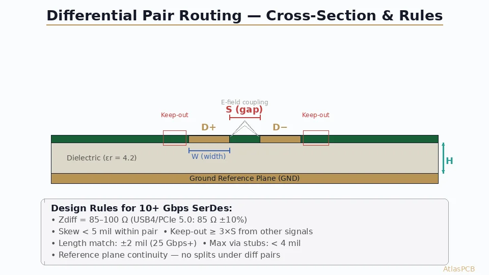
Reference Plane Management
The Cardinal Rule: No Splits Under Differential Pairs
Any discontinuity in the reference plane forces return current to find an alternate path, creating a slot antenna that radiates AND receives interference. Rules:
- Never route high-speed differential pairs over power plane splits
- If crossing between planes is unavoidable, place stitching capacitors (100 pF) within 50 mil of the crossing point
- Use continuous ground planes as reference wherever possible
- Document reference plane assignments on the stackup drawing
Layer Transitions and Return Vias
When a differential pair changes layers (and therefore changes reference plane):
- Place ground stitching vias within 30 mil of the signal vias
- The stitching vias connect the old reference plane to the new one
- Use at least 2 stitching vias (one on each side of the pair)
- Verify the return path is complete with 3D EM simulation for critical interfaces
For comprehensive guidance on signal integrity PCB design, including field solver setup and simulation validation techniques, review our foundational guide.
Crosstalk Management
Near-End Crosstalk (NEXT)
Adjacent differential pairs running in parallel create coupled electromagnetic fields. Managing NEXT:
- Minimum inter-pair spacing: 3× the intra-pair gap (S) for microstrip, 5× for stripline
- Use ground guard traces between pairs when spacing is constrained (ground vias every 200 mil)
- Route on alternating layers — pairs on L3 won’t couple to pairs on L5 with a ground plane between them
Far-End Crosstalk (FEXT)
FEXT is the dominant concern for stripline routing:
- Scales with coupled length — proportional to parallel run distance
- Maximum parallel coupling length: <2 inches at 25 Gbps without detailed analysis
- Stagger routing (offset traces vertically on different layers) to reduce FEXT
Crosstalk Budget
For a typical PCIe 5.0 channel with 20 dB insertion loss budget:
- Total crosstalk allocation: ~3 dB
- Per-aggressor allocation: ~1 dB (assuming 3 adjacent aggressors)
- This translates to isolation requirements of >20 dB across the Nyquist frequency
Connector Breakout Strategies
BGA Escape Routing
Large SerDes-heavy FPGAs and ASICs present the most challenging routing:
- Dog-bone via escape for outer BGA balls (row A/B)
- Inner balls require via-in-pad with filled and capped vias for impedance continuity
- Maintain differential pair spacing through the entire escape — no pinching
- Plan BGA escape on dedicated routing layers with clear reference planes
High-Speed Connector Pads
For PCIe/QSFP/SFP connectors:
- Follow connector manufacturer’s recommended footprint exactly
- Include the specified ground pad pattern for proper impedance
- Anti-pad sizes on internal planes per connector datasheet
- Route breakout at 45° (no 90° bends within 50 mil of pad)
Practical Design Checklist for 25+ Gbps
Use this checklist before releasing Gerbers:
✅ Impedance simulation matches target ±5% across frequency range
✅ Intra-pair length match < 5 mil everywhere
✅ Via stubs back-drilled or eliminated (< 5 mil remaining)
✅ Ground stitching vias within 30 mil of every layer transition
✅ No reference plane splits under any differential pair
✅ Inter-pair spacing ≥ 3× gap width (edge-coupled)
✅ Maximum parallel coupling length documented and within budget
✅ Test coupons specified on panel for impedance verification
✅ Loss budget analysis confirms material supports required channel length
✅ Back-drill depth and tolerance specified in fab drawing
Manufacturing Considerations
To turn these routing rules into working hardware, communicate clearly with your fabricator:
- Specify impedance on the fab drawing — target, tolerance, coupon type (single-ended and differential)
- Provide stackup in the ODB++/IPC-2581 data — don’t rely on the fabricator guessing your intent
- Call out back-drill layers and stubs — specify maximum remaining stub length
- Define material substitution rules — “or equivalent” should specify Dk/Df limits, not just a brand name
Working with a fabricator who has experience in high-layer-count boards and controlled impedance is essential — the manufacturing process variations at these speeds directly impact your signal quality.
Further Reading
- Signal Integrity PCB Design Guide
- PCB Impedance Matching and Differential Pairs
- PCB Impedance Coupon Testing
- High-Speed PCB Material Dk/Df Comparison
- Controlled Impedance PCB Design and Stackup Calculations
Building boards at 25+ Gbps? AtlasPCB specializes in controlled impedance manufacturing with back-drilling, sequential lamination, and TDR verification. We support PCIe 5.0, 400G Ethernet, and USB4 designs with in-house SI expertise. Get your impedance stackup reviewed free →
About AtlasPCB — We specialize in complex PCB manufacturing for HDI, RF, and high-reliability applications. Explore our impedance-controlled PCB manufacturing . Every order includes free engineering review. Get your quote.
Reviewed by AtlasPCB Engineering Team — IPC-certified manufacturing specialists with 15+ years of production experience in HDI, RF, and high-reliability PCB fabrication. Content based on factory floor data and real customer design reviews.
- signal-integrity
- differential-pair
- high-speed-design
- pcie
- serdes