· AtlasPCB Engineering · Engineering · 10 min read
PCB Back Drilling (Controlled-Depth Drilling): Via Stub Removal for 10+ Gbps Signal Integrity
Complete guide to PCB back drilling for via stub removal. Learn stub resonance calculations, drill depth tolerances, IPC specifications, and when back drilling is essential for 10+ Gbps SerDes channels.

Why Via Stubs Kill High-Speed Signals
Every plated through-hole via in a multilayer PCB is a compromise. The drill creates a copper barrel spanning the entire board thickness, but the signal typically only connects on two or three layers. The unused copper barrel extending beyond the last connection is the via stub — and at high data rates, this stub becomes the single most destructive parasitic element in the channel.
The physics are straightforward: a via stub is an unterminated transmission line appendage hanging off the signal path. At the frequency where the stub length equals one quarter wavelength (λ/4), the stub presents a short circuit at the via junction, creating a deep resonant notch in the channel’s frequency response. The signal energy at that frequency — and the harmonics above it — is effectively absorbed and reflected.
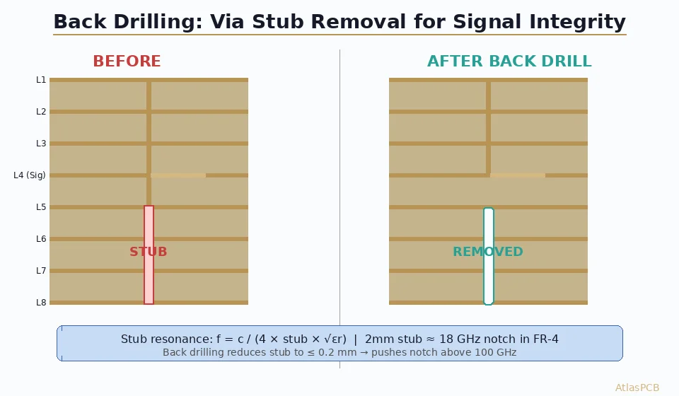
For a 24-layer server board that is 3.2 mm thick, a signal routed on layer 3 that transitions through a through-hole via leaves a stub of roughly 2.8 mm. In FR-4 (εr ≈ 4.0), the first resonant notch frequency is:
f = c / (4 × L_stub × √εr) = 3×10⁸ / (4 × 0.0028 × 2.0) ≈ 13.4 GHz
This falls squarely within the Nyquist bandwidth of [PCIe Gen 5]/blog/differential-pair-routing-rules-high-speed-serdes-pcb/) (16 GHz) and 56G PAM4 channels (14 GHz), making the via unusable without stub removal. Back drilling is the industry-standard solution.
The Mechanics of Back Drilling
How It Works
Back drilling uses a CNC drilling machine with a larger-diameter drill bit (typically 0.2–0.3 mm larger than the original through-hole) to re-enter the via from the opposite side and remove the stub copper. The drill penetrates to a controlled depth, stopping just past the deepest signal connection layer.
The process requires:
- Through-hole drilling and plating — Standard PCB fabrication creates the via barrel
- Controlled-depth re-drilling — A second pass removes the stub portion
- Depth control — Mechanical depth stops, spindle current sensing, or laser measurement ensures the drill stops at the target depth
The remaining stub after back drilling is typically 0.15–0.25 mm (6–10 mil). This residual stub pushes the resonant notch frequency above 100 GHz in FR-4, effectively eliminating it from any practical signal bandwidth.
Drill Parameters
| Parameter | Typical Value | Notes |
|---|---|---|
| Back drill diameter | PTH drill + 0.2–0.3 mm | Ensures complete copper removal |
| Depth tolerance | ±0.1 mm (standard), ±0.05 mm (premium) | CNC with depth sensing |
| Remaining stub | 0.15–0.25 mm | Target above signal layer |
| Entry accuracy | ±0.05 mm XY | Registration to original hole |
| RPM | 40,000–80,000 | Lower than standard drilling |
| Feed rate | 1–2 m/min | Slower for depth control |
Entry Side Selection
The drill enters from the side opposite the signal connection. If the signal connects on layers 2 and 3 (near the top), the back drill enters from the bottom. For signals connecting to deep inner layers, the back drill enters from whichever side yields the shorter travel path to maximize remaining board structural integrity.
Need High-Speed PCBs with Back Drilling?
AtlasPCB delivers production back drilling with ±0.1 mm depth tolerance for 25G/56G/112G SerDes channels. IPC Class 3 certified.
Get a Quote →Stub Resonance: The Quantitative Impact
Resonance Frequency Calculation
The fundamental resonant frequency of a via stub is:
f_res = c / (4 × L_stub × √εr_eff)
Where:
- c = speed of light (3 × 10⁸ m/s)
- L_stub = stub length in meters
- εr_eff = effective dielectric constant of the via environment (typically 3.5–4.2 for FR-4 boards with mixed copper/dielectric)
Harmonics occur at odd multiples: 3f, 5f, 7f — each creating additional notches in the channel response.
Stub Length vs. Resonant Frequency (FR-4, εr ≈ 4.0)
| Stub Length | First Notch | Third Harmonic | Impact on Data Rate |
|---|---|---|---|
| 4.0 mm | 9.4 GHz | 28.1 GHz | Kills 10G+ channels |
| 3.0 mm | 12.5 GHz | 37.5 GHz | Kills 25G+ channels |
| 2.0 mm | 18.8 GHz | 56.3 GHz | Marginal at 25G; kills 56G |
| 1.0 mm | 37.5 GHz | 112.5 GHz | Acceptable for 25G; marginal at 56G |
| 0.5 mm | 75.0 GHz | 225 GHz | Safe for 112G PAM4 |
| 0.2 mm | 187.5 GHz | — | Safe for all current protocols |
Insertion Loss Budget
A via stub does not just create a notch — it degrades insertion loss across the entire bandwidth. Simulations and measurements consistently show:
- 2 mm stub: –3 to –6 dB additional loss at 12.5 GHz
- 1 mm stub: –1 to –2 dB additional loss at 12.5 GHz
- 0.2 mm stub (back drilled): < –0.3 dB at 12.5 GHz
For a 56G PAM4 channel with a total loss budget of –25 to –30 dB, losing 3–6 dB to via stubs consumes 10–24% of the entire budget on a single transition. In a [backplane design]/blog/pcb-backplane-design-high-speed/) with 4+ via transitions per channel, this can easily close the eye completely.
Design Guidelines for Back Drilling
When to Specify Back Drilling
Always required:
- Data rates ≥ 25 Gbps NRZ or 56 Gbps PAM4
- Total board thickness > 2.5 mm with through-hole vias
- Stubs exceeding 1.0 mm on any high-speed signal via
Usually required:
- Data rates 10–25 Gbps NRZ
- Board thickness > 1.6 mm with signals on outer layers through thick vias
- Channels with tight loss budgets (< 5 dB margin)
Rarely needed:
- Data rates < 5 Gbps
- Thin boards (< 1.6 mm) where stubs are inherently short
- Designs using blind/buried vias ([HDI stackup]/blog/hdi-pcb-stackup-design-advanced/))
Design for Manufacturability (DFM) Rules
Back drill diameter = PTH finished hole diameter + 0.2 mm minimum (0.3 mm preferred). This ensures the entire copper barrel is removed even with registration tolerance.
Annular ring clearance — The back-drilled hole will be larger than the original, so ensure non-functional pads on back-drilled layers have sufficient clearance to avoid unintended shorts.
Minimum remaining stub — Specify 0.2 mm (8 mil) minimum remaining stub to provide a safety margin. Going below 0.15 mm risks drilling into the signal layer.
Via pad removal — On layers where the via stub has been removed, the copper pad no longer serves any electrical purpose. Remove non-functional pads (NFPs) in the design to reduce capacitive loading. This is complementary to back drilling and further improves impedance continuity.
Drill from the correct side — Clearly indicate in your [fabrication drawing]/blog/pcb-fabrication-tolerance-guide/) which vias require back drilling, the entry side, and the target depth. Use a separate drill table or note.
Stackup Optimization
The most effective approach combines back drilling with intelligent layer assignment:
- Route high-speed signals on layers near the entry surface (top or bottom layers 1–4) to minimize stub length even before back drilling
- Place power and ground planes in the middle of the stackup where via stubs are longest — these nets are not sensitive to stubs
- If signals must connect to deep inner layers, consider using blind vias (HDI technology) rather than through-hole vias with back drilling
For a [16-layer stackup]/blog/16-layer-pcb-stackup-design/), routing 25G signals on layers 2–3 with back drilling from the bottom leaves a residual stub of ~0.2 mm instead of the 2+ mm stub of a through-hole via.
Back Drilling vs. Alternative Stub Mitigation
Comparison with Blind/Buried Vias
| Characteristic | Back Drilling | Blind/Buried Vias |
|---|---|---|
| Cost premium | 5–15% | 30–100%+ |
| Stub elimination | Residual 0.1–0.25 mm | Zero (inherent) |
| Board thickness | Any | Sequential lamination limits |
| Layer count limit | None practical | Complex above 6+ sequential builds |
| Process maturity | Very mature | Mature for standard HDI |
| Design flexibility | Post-layout applied | Must plan in stackup design |
| Reliability | Well understood | Depends on [microvia reliability]/blog/hdi-microvia-stacked-vs-staggered-reliability/) |
Comparison with Via-in-Pad (VIPPO)
Via-in-pad with plating over (VIPPO) addresses component mounting, not stub removal. A [VIPPO via]/blog/bga-pad-design-via-in-pad-solder-voiding-prevention/) still creates a stub if it is a through-hole via. The two techniques are complementary — a BGA pad can use VIPPO for solder joint integrity and back drilling for signal integrity.
Impedance-Controlled Back Drilling
For the most critical applications (112G SerDes, 800G Ethernet), some designers specify anti-pad optimization around the back-drilled via to maintain [controlled impedance]/blog/controlled-impedance-pcb-design-stackup-calculations/) through the entire via transition. This involves:
- Optimizing the anti-pad diameter on each layer
- Matching the via barrel impedance to the trace impedance (typically 85–100 Ω differential)
- Using 3D electromagnetic simulation to verify the via transition insertion loss and return loss
Fabrication Process Control
Depth Measurement Methods
Production back drilling uses three primary depth control methods:
Mechanical depth stop — The drill spindle has a physical stop that limits penetration depth. Accuracy: ±0.15 mm. Used for standard applications.
Spindle current monitoring — The CNC machine monitors spindle motor current, detecting the higher resistance when the drill transitions from air/plating to laminate. Accuracy: ±0.1 mm. Most common production method.
Laser/optical depth sensing — An integrated laser measures the board surface height before drilling and tracks depth in real-time. Accuracy: ±0.05 mm. Used for premium applications like 56G/112G backplanes.
Quality Verification
Back drill quality is verified through:
- Cross-section (microsection) — The gold standard. A cross-section through a back-drilled via reveals the actual remaining stub length, copper removal completeness, and any damage to adjacent layers. Per [IPC-A-600]/blog/ipc-a-600-pcb-acceptability-inspection-guide/) acceptance criteria.
- Stub measurement via TDR — Time-domain reflectometry on a test coupon with back-drilled vias confirms the electrical stub length matches the mechanical specification.
- X-ray inspection — Non-destructive verification of drill depth and centering on the via.
Common Defects
| Defect | Cause | Prevention |
|---|---|---|
| Over-drilling (signal damage) | Depth control error | Increase safety margin to 0.25 mm; use laser depth sensing |
| Under-drilling (excessive stub) | Board thickness variation | Measure actual board thickness per panel |
| Off-center drilling | Registration error | Verify alignment targets; use ±0.05 mm capable equipment |
| Copper burrs at drill exit | Dull bit or incorrect feed | Fresh drill bits; optimize feed/speed ratio |
| Delamination at drill bottom | Excessive heat | Reduce RPM and feed rate for deep back drills |
IPC Specifications and Industry Standards
IPC-6012 Requirements
IPC-6012 (Qualification and Performance Specification for Rigid Printed Boards) addresses back drilling under the controlled-depth drilling provisions:
- Class 2 (standard): Depth tolerance per manufacturer’s capability, typically ±0.15 mm
- Class 3 (high reliability): Tighter tolerance per drawing requirements, typically ±0.1 mm
- Remaining copper: No specification on minimum — per design requirements
- Copper removal: Must be complete within the back drill diameter
Fabrication Drawing Callouts
Your fabrication notes should specify:
BACK DRILL REQUIREMENTS:
- Via IDs: BD1, BD2 (as referenced in drill table)
- Entry side: Bottom (or as noted per via)
- Target depth: X.XX mm from entry surface (±0.10 mm)
- Remaining stub: 0.20 mm max above [signal layer]
- Back drill diameter: Original hole + 0.25 mm
- Coupon verification: Cross-section per IPC-TM-650, Method 2.1.1
Practical Example: 56G PAM4 Backplane
Consider a 20-layer backplane, 3.5 mm thick, with 56G PAM4 lanes routed on layers 3–4:
Without back drilling:
- Stub length: ~2.8 mm (layers 5 through 20)
- First resonant notch: ~13.4 GHz
- 56G PAM4 Nyquist: 14 GHz
- Result: Notch falls directly in signal bandwidth — channel fails
With back drilling:
- Remaining stub: 0.2 mm
- First resonant notch: ~187 GHz
- Result: No impact on signal bandwidth — channel passes with margin
Loss improvement at 14 GHz:
- Without back drilling: –5.2 dB per via transition
- With back drilling: –0.8 dB per via transition
- Savings per via pair: 4.4 dB × 4 transitions = 17.6 dB channel budget recovered
That 17.6 dB is often the difference between a passing and failing channel.
Cost and Lead Time Impact
Back drilling adds modest cost and lead time to the PCB fabrication process:
- Cost premium: 5–15% of bare board cost (depends on number of back-drilled holes)
- Lead time: Adds 0.5–1 day to the fabrication cycle
- NRE: Requires a separate NC drill program — most fabricators include this in the setup
- Yield impact: Minimal for experienced fabricators (< 1% scrap rate)
Compared to the alternatives — sequential lamination for blind vias (30–100% cost premium) or accepting channel failures — back drilling delivers the best performance-to-cost ratio for high-speed through-hole via applications.
Further Reading
- [Differential Pair Routing Rules for 10+ Gbps SerDes]/blog/differential-pair-routing-rules-high-speed-serdes-pcb/)
- [High-Speed Backplane PCB Design]/blog/pcb-backplane-design-high-speed/)
- [Controlled Impedance PCB Stackup Design]/blog/controlled-impedance-pcb-design-stackup-calculations/)
- [PCB Controlled-Depth Drilling Explained]/blog/pcb-controlled-depth-drilling/)
- [IPC-A-600 Acceptability Standard]/blog/ipc-a-600-pcb-acceptability-inspection-guide/)
Need back-drilled PCBs for your 25G, 56G, or 112G designs? Contact AtlasPCB Engineering for a fast quote. We deliver production back drilling with ±0.1 mm depth tolerance and full cross-section verification on every lot.
About AtlasPCB — We specialize in complex PCB manufacturing for HDI, RF, and high-reliability applications. Explore our impedance-controlled PCB manufacturing . Every order includes free engineering review. Get your quote.
Reviewed by AtlasPCB Engineering Team — IPC-certified manufacturing specialists with 15+ years of production experience in HDI, RF, and high-reliability PCB fabrication. Content based on factory floor data and real customer design reviews.
- signal-integrity
- back-drilling
- high-speed-design
- via-design
- pcb-fabrication
- manufacturing