· AtlasPCB Engineering · Engineering · 7 min read
Signal Return Path and Ground Via Stitching in High-Speed PCB Design
Understanding signal return paths and ground via stitching for high-speed PCB design. Learn λ/20 spacing rules, reference plane transitions, and EMI reduction strategies.

The Physics of Return Current
Every current needs a complete circuit. When a signal propagates along a PCB trace, an equal-and-opposite return current flows on the nearest reference plane (ground or power plane). This isn’t a design choice — it’s physics. Maxwell’s equations dictate that AC return current follows the path of least impedance, which at high frequencies means directly beneath the signal trace on the adjacent plane.
Understanding this principle is fundamental to high-speed PCB design because:
- Disrupting the return path creates impedance discontinuities
- Return current loops radiate electromagnetic interference
- Split planes force return current to find alternative paths
- Layer transitions without stitching vias break return continuity
Return Current Behavior at Different Frequencies
Low Frequency (< 100 kHz)
At low frequencies, return current follows the path of least resistance. It spreads across the entire ground plane, taking the shortest geometric path between source and load. The current density is relatively uniform.
High Frequency (> 1 MHz)
At high frequencies, return current follows the path of least inductance — which is directly beneath the signal trace. The current concentrates in a narrow band (approximately 3× trace width) on the reference plane. This behavior creates a tightly-coupled transmission line with predictable impedance.
The Transition Region
Between 100 kHz and 1 MHz, current distribution transitions from resistance-dominated to inductance-dominated spreading. The skin depth at 1 MHz in copper is approximately 66μm, meaning return current is confined to the top surface of the reference plane facing the signal trace.
Reference Plane Continuity
Why Plane Splits Are Dangerous
A split or void in the reference plane directly beneath a signal trace forces return current to detour around the gap. This creates:
- Impedance discontinuity — characteristic impedance spikes at the gap
- Radiation — the detour path forms a loop antenna proportional to gap size
- Crosstalk — return current from one signal couples to adjacent signal returns
- Common-mode noise — asymmetric return path generates CM currents
Rules for Reference Plane Design
- Never route high-speed signals over plane splits — if a split is necessary, route signals on layers that reference a continuous plane
- Bridge capacitors across splits — place 100nF capacitors (0402) every 5mm across power plane splits that carry return current
- Avoid via anti-pads that create gaps — use smaller anti-pad diameters (0.5mm) to maintain plane continuity near critical signals
- Use dedicated return planes — in 6+ layer stackups, dedicate at least two layers as continuous ground planes
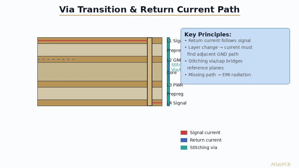
Layer Transitions and Stitching Vias
The Problem: Signal Via Without Return Via
When a signal transitions from Layer 1 (referenced to GND on Layer 2) to Layer 4 (referenced to GND on Layer 5), the return current must also transition from Layer 2 to Layer 5. Without a nearby ground via connecting these planes, the return current must:
- Spread laterally across Layer 2
- Find a distant connection between the ground planes
- Travel back to the signal via location on Layer 5
- Reconcentrate beneath the signal trace
This creates a large current loop — measured in centimeters rather than millimeters — that radiates effectively at frequencies where the loop dimension approaches λ/4.
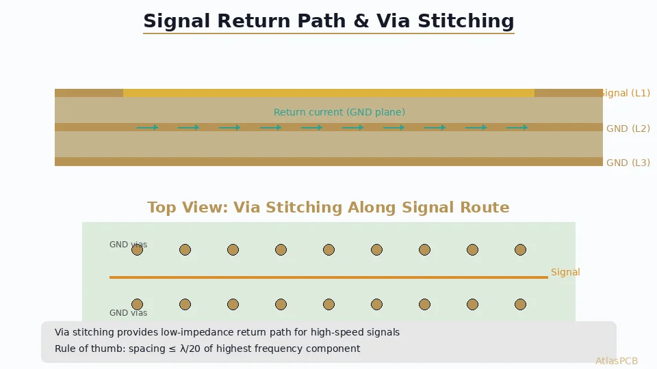
The Solution: Stitching Vias
A stitching via placed adjacent to the signal via provides a low-impedance path for return current between reference planes. The return current transitions cleanly within < 1mm of the signal via, maintaining the tight coupling that preserves controlled impedance.

Complex High-Speed Stackup? We Handle Signal Integrity.
AtlasPCB manufactures controlled-impedance boards up to 40 layers with ±7% impedance tolerance. Our DFM review identifies return path issues before fabrication.
Get Your Impedance-Controlled Quote →Ground Via Stitching Design Rules
Spacing Calculation: The λ/20 Rule
Maximum stitching via spacing should not exceed λ/20 at the highest significant frequency:
Maximum spacing = c / (20 × f × √εr_eff)

Where:
  c = speed of light (3 × 10⁸ m/s)
  f = highest significant frequency (GHz)
  εr_eff = effective dielectric constant (≈ 3.5 for FR-4)
Examples:
| Signal Data Rate | f_knee (GHz) | λ/20 in FR-4 | Max Via Spacing |
|---|---|---|---|
| 1 Gbps NRZ | 0.5 | 16mm | 16mm |
| 5 Gbps NRZ | 2.5 | 3.2mm | 3.2mm |
| 10 Gbps NRZ | 5.0 | 1.6mm | 1.6mm |
| 28 Gbps NRZ | 14 | 0.57mm | 0.57mm |
| 56 Gbps PAM4 | 14 | 0.57mm | 0.57mm |
The f_knee is calculated as 0.5/t_rise for NRZ signals, where t_rise is the 10-90% rise time.
Stitching Via Placement Near Signal Vias
For each signal layer transition:
Basic rule (< 3 GHz):
- One stitching via within 50mil (1.27mm) of signal via
- Connected to both reference planes (source and destination)
Moderate speed (3-10 GHz):
- One or two stitching vias within 20mil (0.5mm)
- Place on the side of the signal via closest to the ground plane connection
High speed (> 10 GHz):
- Two stitching vias flanking the signal via, within 15mil (0.38mm)
- For differential pairs: stitching vias between and outside the P/N pair
- Consider via stub length — back-drill if stub > λ/8
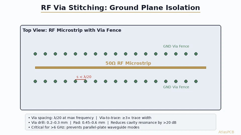
Perimeter Stitching
Board edges without stitching vias act as slot antennas. Place perimeter ground vias:
- Along all board edges at λ/20 spacing
- Around all connector mounting areas
- Surrounding high-speed IC packages (create a via cage)
- Along the boundary between analog and digital sections
Differential Pair Layer Transitions
Differential pairs require special attention during layer transitions:
Symmetry Requirements
Both P and N vias must transition through identical via structures:
- Same drill diameter
- Same pad size
- Same anti-pad clearance
- Symmetrical stitching via placement
- Equal via stub lengths (back-drill both identically)
Stitching Via Configuration
For differential pairs at > 5 Gbps:
Layout pattern (top view):

  GND_via    P_via    GND_via    N_via    GND_via
     ○         ●         ○         ●         ○

GND vias: 0.3mm drill, standard anti-pad
Spacing: P-to-N maintained through via transition
This five-via pattern ensures symmetric return paths for both polarities of the differential signal.
EMI Consequences of Poor Return Path Design
Quantifying Radiation
A current loop radiates with field strength proportional to:
E ∝ f² × I × A

Where:
  f = frequency of interest
  I = current amplitude
  A = loop area (cm²)
A 10× reduction in loop area (from 10cm² to 1cm²) reduces radiated emissions by 20 dB. This is why proper stitching via placement — reducing return current loop area from centimeters to sub-millimeter — is the single most effective EMI mitigation strategy.
Failing EMC Compliance
Common FCC/CISPR failures traced to return path issues:
- Narrowband spikes at clock harmonics — clock signal vias without stitching
- Broadband emissions 30-300 MHz — signals crossing plane splits
- Cable common-mode radiation — connector ground vias missing stitching
Advanced Topics
Via Stitching in Mixed-Signal Designs
When analog and digital ground planes must be separate:
- Stitch only at the single-point connection (typically at ADC/DAC)
- Use a solid ground plane beneath both sections where possible
- Route analog signals exclusively over the analog reference plane
- Guard traces with stitched ground on both sides
Stitching in Cavity-Backed Antenna PCBs
For RF PCBs with integrated patch antennas:
- Dense via fencing (λ/10 spacing) around antenna cavity
- Do NOT stitch through the antenna element area
- Stitching via rows create a waveguide-below-cutoff fence
Power Plane as Return Path
When a signal references a power plane instead of ground:
- The power plane still carries return current at AC (decoupled to ground via capacitors)
- Place decoupling capacitors near signal via transitions
- Via stitching connects power plane to ground plane through decoupling network
Practical Design Checklist
✅ Every signal via has at least one stitching via within 0.5mm
✅ Stitching via spacing along board edges ≤ λ/20 at f_knee
✅ No high-speed traces cross plane splits or voids
✅ Differential pair transitions maintain P/N symmetry
✅ Via anti-pads don’t create gaps in return current path
✅ Decoupling capacitors placed near power-referenced signal transitions
✅ Back-drilling applied where via stubs exceed λ/8
✅ Via cage surrounds high-speed BGA devices
Further Reading
- PCB Ground Plane Design: EMI and Ground Bounce Reduction
- Controlled Impedance PCB Stackup Design Rules
- PCB Back-Drilling for Via Stub Removal and Signal Integrity
- EMC Shielding: PCB Via Fence and Ground Plane Design
Designing a high-speed board with complex layer transitions? AtlasPCB offers controlled-impedance manufacturing with ±7% tolerance and back-drilling services. Our SI engineering team reviews every design for return path integrity. Start your project →
About AtlasPCB — We specialize in complex PCB manufacturing for HDI, RF, and high-reliability applications. Explore our impedance-controlled PCB manufacturing . Every order includes free engineering review. Get your quote.
Reviewed by AtlasPCB Engineering Team — IPC-certified manufacturing specialists with 15+ years of production experience in HDI, RF, and high-reliability PCB fabrication. Content based on factory floor data and real customer design reviews.
- signal return path
- via stitching
- ground plane
- high-speed PCB
- EMI
- signal integrity
- reference plane