· AtlasPCB Engineering · Engineering · 11 min read
Controlled Impedance PCB Stackup Design: Rules, Calculations, and Manufacturing Tolerances for High-Speed Designs
Master controlled impedance PCB stackup design with practical rules for microstrip, stripline, and differential pair geometries. Covers impedance calculation methods, manufacturing tolerances, and material selection for designs from 1 Gbps to 112 Gbps PAM4.

Introduction: Why Impedance Control Defines Modern PCB Design
Every signal above a few hundred megahertz behaves as a transmission line. When the signal’s rise time creates wavelengths comparable to the trace length, controlled impedance stops being optional and becomes the single most important aspect of your PCB stackup design.
Get impedance wrong, and you’ll see reflections, ringing, eye diagram degradation, and bit errors — problems that no amount of post-layout tuning can fix. Get it right, and your 56 Gbps PAM4 channels work on the first spin.
This guide covers the complete workflow for designing controlled impedance stackups: from understanding the physics, through practical calculation methods, to manufacturing specifications that ensure your fabricator delivers what your simulation predicted.
Understanding Transmission Line Fundamentals
What Determines Impedance?
Characteristic impedance (Z₀) of a PCB trace depends on four geometric and material properties:
- Trace width (W) — wider traces = lower impedance
- Dielectric thickness (H) — distance to reference plane; thicker = higher impedance
- Dielectric constant (Dk/εr) — higher Dk = lower impedance
- Copper thickness (T) — thicker copper slightly reduces impedance
The relationship is approximately:
Z₀ ∝ √(L/C) ∝ (H/W) × (1/√Dk)This means impedance is fundamentally a ratio of height-to-width scaled by the dielectric properties. Understanding this ratio relationship is key to intuitive stackup design.
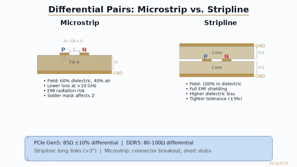
Microstrip vs. Stripline
Microstrip (outer layers):
- Trace on surface with one reference plane below
- Effective Dk is ~60-70% of laminate Dk (field partially in air)
- Soldermask increases effective Dk by 0.3-0.5
- Higher loss due to radiation and surface roughness exposure
- Easier to probe and debug
Stripline (inner layers):
- Trace sandwiched between two reference planes
- Full laminate Dk applies (field entirely in dielectric)
- Lower radiation loss, better EMC performance
- Required for high-speed differential pairs above 10 Gbps
- Cannot be directly probed
Differential Pairs:
- Two coupled traces carrying complementary signals
- Differential impedance (Zdiff) ≈ 2 × Zodd ≈ 2 × Z₀ × (1 - coupling factor)
- Tighter coupling (smaller spacing) reduces differential impedance
- Typical targets: 85Ω (USB 3.x), 100Ω (PCIe, Ethernet), 90Ω (HDMI)
Stackup Architecture for Impedance Control
The Reference Plane Rule
Every signal trace must have a continuous, unbroken reference plane on an immediately adjacent layer. This is non-negotiable for controlled impedance.
Violations of this rule — signal layers adjacent to other signal layers, split planes, or reference plane gaps — create impedance discontinuities that no amount of trace width adjustment can fix.
Standard Stackup Configurations
4-Layer (Standard):
L1: Signal (microstrip) — references L2
L2: Ground plane
L3: Power plane
L4: Signal (microstrip) — references L3- Good for: designs < 5 Gbps, moderate pin count
- Limitation: only 2 routing layers, inner signals not possible
6-Layer (Recommended for high-speed):
L1: Signal (microstrip)
L2: Ground plane
L3: Signal (stripline) — references L2 and L4
L4: Power/Ground plane
L5: Signal (stripline) — references L4 and L6
L6: Ground plane → Signal (microstrip)- Good for: PCIe Gen 4/5, USB 3.x, moderate channel lengths
8-Layer (High-performance):
L1: Signal (microstrip)
L2: Ground plane
L3: Signal (stripline)
L4: Ground plane
L5: Power plane
L6: Signal (stripline)
L7: Ground plane
L8: Signal (microstrip)- Every signal layer has dedicated adjacent reference planes
- Ideal for: 25G+ SerDes, dense routing, EMC-sensitive designs
Dielectric Thickness Planning
Work with your fabricator’s standard prepreg and core thicknesses. Common options:
| Material | Thickness (mil) | Typical Use |
|---|---|---|
| 1080 prepreg | 2.8-3.2 | Thin dielectric for high-impedance traces |
| 2116 prepreg | 4.5-5.0 | Standard signal-to-plane spacing |
| 1080×2 prepreg | 5.5-6.0 | Moderate spacing |
| 7628 prepreg | 7.0-7.5 | Thick spacing for wide 50Ω microstrip |
| Core | 3.0-40.0 | Structural stability |
Critical insight: You don’t choose a dielectric thickness and calculate the resulting trace width. You target a standard trace width (4, 5, 6, 7, or 8 mil) and select the prepreg/core combination that achieves your target impedance at that width.
Impedance Calculation Methods
Why Formulas Aren’t Enough
Classic formulas (IPC-2141, Wadell) provide estimates within 5-15% but miss critical real-world factors:
- Trapezoidal trace cross-section (etch factor narrows top surface)
- Soldermask coating (adds 0.3-0.5 to effective Dk)
- Copper roughness (Rz affects Dk at >5 GHz)
- Dk frequency dependence (Dk drops 5-10% from 1 GHz to 20 GHz)
- Resin content variation in woven glass prepregs
Field Solver Approach (Recommended)
Modern 2D field solvers numerically compute impedance by solving Maxwell’s equations for your exact cross-sectional geometry:
Tools:
- Polar SI9000 — Industry standard, includes fabricator databases
- Saturn PCB Toolkit — Free, excellent for initial estimates
- Altium/Cadence built-in — Integrated with layout tools
- Simbeor — Advanced for frequency-dependent analysis
Input parameters for accurate results:
- Trace width (bottom/top for trapezoidal)
- Copper thickness (including plating)
- Dielectric thickness (specify per layer)
- Material Dk at target frequency
- Soldermask thickness and Dk (for microstrip)
- Adjacent trace coupling (for differential pairs)
Etch Factor Compensation
PCB etching creates a trapezoidal cross-section: the trace is wider at the base than at the top. Typical etch factors:
- 1 oz copper: top width = bottom width - 0.5 mil per side (1.0 mil total)
- 0.5 oz copper: top width = bottom width - 0.3 mil per side
- 2 oz copper: top width = bottom width - 1.0 mil per side
Always specify trace width at the base (wider dimension) in your Gerber files, as this is what the fabricator’s artwork defines. The field solver should model the trapezoidal shape for accurate impedance prediction.
Need Impedance-Controlled PCBs?
AtlasPCB provides ±10% impedance control with TDR verification on every production panel. Our engineers review your stackup before fabrication.
Get a Stackup Review →Material Selection for Impedance Control
Dk Stability: The Hidden Variable
Not all FR-4 is equal. The Dk value of “FR-4” can range from 3.8 to 4.8 depending on:
- Resin content: Higher resin = lower Dk (resin Dk ≈ 3.2, glass Dk ≈ 6.2)
- Glass style: 1080 (65% resin) vs. 7628 (45% resin) significantly affects Dk
- Frequency: Dk decreases 5-10% from 100 MHz to 10 GHz
- Moisture: Absorbed water (Dk=80) raises effective Dk
For controlled impedance, always specify the exact prepreg style, not just “FR-4.”
Material Tiers for Different Speed Classes
Standard FR-4 (Dk≈4.2, Df≈0.020)
- Suitable: <3 Gbps, short channels <6 inches
- Examples: Shengyi S1000-2, ITEQ IT-180A
Mid-loss (Dk≈3.6-3.8, Df≈0.005-0.010)
- Suitable: 5-28 Gbps, channels 6-20 inches
- Examples: Panasonic Megtron 4, Isola Tachyon-100G, Shengyi S1000-2M
Ultra-low-loss (Dk≈3.2-3.5, Df≈0.002-0.004)
- Suitable: 56-112 Gbps PAM4, channels >10 inches
- Examples: Panasonic Megtron 7, Isola I-Speed, Rogers RO4000 series
Dk Tolerance Specification
| Material Grade | Dk Tolerance | Impact on 50Ω Impedance |
|---|---|---|
| Standard FR-4 | ±0.15-0.25 | ±3-5% variation |
| Controlled Dk FR-4 | ±0.05-0.10 | ±1-2% variation |
| High-frequency laminate | ±0.02-0.05 | <±1% variation |
For ±5% impedance tolerance, you need material with Dk tolerance ≤±0.10. Standard FR-4’s wider Dk range means ±10% impedance tolerance is the practical achievable limit.
Manufacturing Tolerances and Specifications
What to Specify on Your Fabrication Drawing
Your impedance control note should include:
CONTROLLED IMPEDANCE REQUIREMENTS:
- Single-ended: 50Ω ±10% (Layers 1, 4, 5, 8)
- Differential: 100Ω ±10% (Layers 3, 6)
- Reference: Adjacent ground planes as shown in stackup
- Verification: TDR coupon measurement per IPC-2141
- Report: Provide impedance test report with shipment
Critical Manufacturing Tolerances
| Parameter | Standard | Premium |
|---|---|---|
| Trace width | ±0.75 mil | ±0.5 mil |
| Dielectric thickness | ±10% | ±5% (±0.5 mil) |
| Copper thickness | ±20% | ±10% |
| Registration | ±3 mil | ±2 mil |
| Etch factor | Controlled | Controlled + verified |
TDR Verification
Time Domain Reflectometry (TDR) measures actual impedance of fabricated test coupons:
- Coupon design: Include impedance coupons in panel margin (same layer, same trace geometry)
- Measurement points: At least 3 points per coupon (start, middle, end)
- Acceptance criteria: All points within specified tolerance band
- Documentation: Request impedance test report with every lot
Important: Coupon impedance ≠ board impedance if your board has different copper density affecting etch rates. For critical designs, request coupons with similar surrounding copper density.
Design Rules for Common Interfaces
PCIe Gen 5/6 (32/64 GT/s)
- Differential impedance: 85Ω ±10%
- Material: Megtron 4 minimum, Megtron 6 for Gen 6
- Intra-pair skew: <2.5 mil/inch
- Max channel loss: 28 dB at Nyquist (Gen 5), 36 dB (Gen 6)
- Reference plane: continuous, no splits or voids under pairs
USB 3.2/4 (10/20/40 Gbps)
- Differential impedance: 90Ω ±10%
- Material: standard FR-4 adequate for USB 3.2, low-loss for USB4
- Intra-pair skew: <5 mil/inch
- Length matching: ±5 mil within pair
100G/400G Ethernet (25.78G/53.125G per lane)
- Differential impedance: 100Ω ±10%
- Material: Megtron 6/7 for backplane, Megtron 4 for line card
- Via stub length: <5 mil (back-drill required)
- Total channel insertion loss budget: 28-35 dB
DDR5 (4800-8800 MT/s)
- Single-ended impedance: 40Ω (DQ), 48Ω (command/address)
- Differential impedance: 80Ω (clock)
- Material: standard FR-4 adequate for DDR5-5600, mid-loss for DDR5-8800
- Length matching: within byte lane ±25 mil, clock to DQS ±5 mil
Advanced Topics
Impedance Discontinuities at Vias
Every via is an impedance discontinuity. A standard through-hole via (drill 10 mil, pad 20 mil, antipad 30 mil) presents approximately 25-35Ω impedance — a massive mismatch against 50Ω or 100Ω targets.
Mitigation strategies:
- Back-drilling: Remove unused via stub to reduce capacitance (essential for >10 Gbps)
- Via optimization: Size antipad to achieve ~50Ω via impedance (typically 35-45 mil antipad)
- Blind/buried vias: Eliminate stubs entirely for [HDI designs]/blog/hdi-microvia-stacked-vs-staggered-reliability-en/)
Fiber Weave Effect
Woven glass cloth creates periodic Dk variations across the board surface. When differential pair traces align differently relative to the weave pattern, one trace experiences higher Dk than its partner, causing intra-pair skew.
Mitigation:
- Route at angles offset from fiber weave (not exactly 0° or 90°)
- Use spread glass or flat glass prepregs (NE-glass, 2×1080 instead of 1×2116)
- Specify “controlled impedance grade” glass styles from your laminate supplier
Temperature Effects
Dk typically decreases 200-400 ppm/°C for FR-4 materials. Over a -40°C to +85°C operating range, this produces approximately:
- ±1.5% Dk variation for standard FR-4
- ±0.5% Dk variation for Rogers/PTFE
This translates to ±0.7% impedance change for FR-4, which is generally negligible compared to manufacturing tolerances.
Stackup Design Workflow
Step 1: Define Requirements
- List all impedance targets (interface specifications)
- Determine layer count (routing complexity + signal integrity)
- Select material grade (speed class + channel length)
Step 2: Initial Stackup Proposal
- Assign signal and reference plane layers
- Choose initial prepreg/core thicknesses from fabricator’s available stock
- Target standard trace widths (4, 5, or 6 mil for inner, 5-8 mil for outer)
Step 3: Field Solver Optimization
- Model each impedance geometry in field solver
- Adjust dielectric thickness to hit targets at preferred trace width
- Verify differential impedance with actual pair spacing
- Include soldermask effect for outer layers
Step 4: Fabricator Review
- Send proposed stackup to fabricator for DFM review
- Fabricator confirms material availability and achievable tolerances
- Iterate if needed (different prepreg combinations, adjusted thicknesses)
Step 5: Verification Specification
- Define TDR coupon geometry matching your critical traces
- Specify impedance tolerance and testing requirements
- Include impedance specification on fabrication drawing
Common Mistakes and How to Avoid Them
Mistake 1: Ignoring Soldermask
Soldermask adds 0.5-1.0 mil of dielectric over outer-layer traces with Dk ≈ 3.5-4.0. This increases microstrip impedance by 2-5Ω. Always include soldermask in your impedance simulation.
Mistake 2: Assuming FR-4 Dk = 4.0
Generic “FR-4 Dk=4.0” is a dangerous simplification. Actual Dk depends on prepreg style, resin content, and frequency. Always use the specific prepreg’s datasheet Dk value.
Mistake 3: Forgetting Plating Thickness
Outer layers receive 0.5-1.5 mil of electroless + electrolytic copper plating. This increases total copper thickness and slightly affects impedance. Specify “finished copper thickness” to your fabricator.
Mistake 4: Reference Plane Splits
A ground plane split under a signal trace creates an impedance discontinuity and forces return current to detour around the split. Never route controlled impedance traces across plane splits. If a plane change is necessary, add stitching vias to provide return current path.
Mistake 5: Not Back-Drilling
For designs above 5 Gbps, through-hole via stubs create resonant structures that produce notches in the frequency response. A 60-mil stub creates a quarter-wave resonance at approximately 12.5 GHz — right in the middle of 25G signal bandwidth. Always specify back-drilling for high-speed vias.
Working with Your Fabricator
Early Engagement Is Essential
Don’t finalize your stackup in isolation. Fabricators have:
- Specific prepreg inventories — your ideal stackup may require non-stocked materials
- Process capabilities — trace/space minimums, drill aspect ratios, back-drill accuracy
- Impedance modeling experience — they know which specifications are achievable
Questions to Ask Your Fabricator
- What prepreg styles do you stock for my target Dk?
- What dielectric thickness tolerance can you hold?
- What is your etch factor for my copper weight on inner/outer layers?
- Do you back-drill, and what’s your stub length accuracy?
- Can I get pre-production impedance verification before full lot?
Conclusion: Impedance Is a Partnership
Controlled impedance isn’t something you design alone — it’s a manufactured outcome that requires collaboration between designer and fabricator. The designer defines the requirements and geometry; the fabricator delivers the physical reality within agreed tolerances.
Start with your interface specifications, select appropriate materials for your speed class, model the cross-sections in a field solver, and engage your fabricator early. With this approach, achieving ±10% impedance control is routine, and even ±5% is achievable for critical applications.
Ready for impedance-controlled PCB fabrication? AtlasPCB provides complimentary stackup review for all impedance-controlled designs. Our signal integrity engineers verify your field solver assumptions against our manufacturing process data, ensuring first-pass success.
Get Your Stackup Reviewed → | View Our Impedance Control Capabilities →
Further Reading
- [PCB Manufacturer with Engineering Review: Why Human DFM Audit Matters]/blog/pcb-manufacturer-engineering-review/)
- [Controlled Impedance PCB Design: Stack-Up Calculations, Tolerance Analysis, and Manufacturing Guide]/blog/controlled-impedance-pcb-design-stackup-calculations/)
- [Aluminum PCB Thermal Design for High-Power LED and Motor Drivers: Material Selection, Stackup, and DFM Guide]/blog/aluminum-pcb-thermal-design-led-motor-driver/)
- [AI Hardware PCB Thermal Management: Advanced Multilayer Stackup Design for 1000W+ Processing Units]/blog/ai-hardware-pcb-thermal-management-multilayer-design/)
- [PCB Manufacturing Process: 15 Steps from Gerber to Finished Board]/blog/pcb-manufacturing-process-15-steps/)
- Rigid PCB Manufacturing
About AtlasPCB — We specialize in complex PCB manufacturing for HDI, RF, and high-reliability applications. Explore our RF and high-frequency PCB services, or get an impedance-controlled PCB manufacturing . Every order includes free engineering review. Get your quote.
Reviewed by AtlasPCB Engineering Team — IPC-certified manufacturing specialists with 15+ years of production experience in HDI, RF, and high-reliability PCB fabrication. Content based on factory floor data and real customer design reviews.
- controlled impedance
- PCB stackup
- signal integrity
- microstrip
- stripline
- differential pair
- high-speed PCB