· AtlasPCB Engineering · Engineering · 8 min read
Signal Reflections and Impedance Mismatch on PCBs: Termination Strategies for High-Speed Design
Understand how impedance discontinuities cause signal reflections, ringing, and overshoot on PCB transmission lines. Learn series, parallel, Thevenin, and AC termination techniques with design equations and practical layout guidelines for multi-gigabit interfaces.
The Physics of Signal Reflections
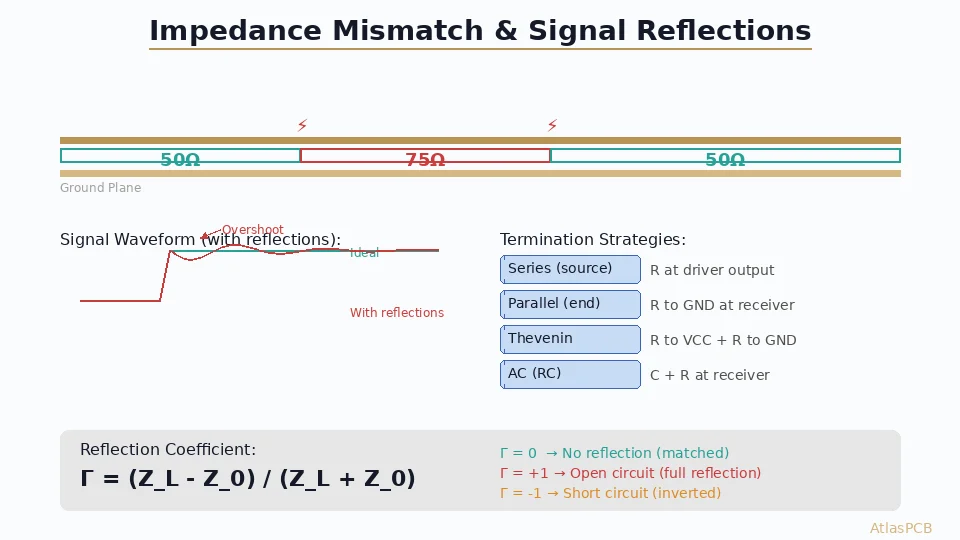
When an electrical signal propagates along a PCB transmission line, it travels as an electromagnetic wave in the dielectric between the trace and its reference plane. The characteristic impedance Z0 of this transmission line depends on geometry — trace width, dielectric thickness, and copper weight. As long as Z0 remains constant, the signal propagates cleanly from source to load.
The moment the signal encounters a point where Z0 changes — a wider trace, a via, a connector, or a load impedance different from Z0 — part of the signal energy reflects back toward the source. This is governed by the fundamental reflection equation:
Γ = (Z_L - Z_0) / (Z_L + Z_0)
Where:
- Γ = reflection coefficient (-1 to +1)
- Z_L = impedance at the discontinuity
- Z_0 = characteristic impedance of the incoming line
The reflected signal amplitude equals Γ times the incident signal amplitude. The transmitted signal amplitude equals (1 + Γ) times the incident amplitude.
Physical Consequences of Reflections
| Γ Value | Condition | Result |
|---|---|---|
| 0 | Perfect match (Z_L = Z_0) | No reflection, full transmission |
| +1 | Open circuit (Z_L = ∞) | Full positive reflection |
| -1 | Short circuit (Z_L = 0) | Full inverted reflection |
| +0.2 | Mild mismatch (Z_L > Z_0) | 20% overshoot at load |
| -0.2 | Mild mismatch (Z_L < Z_0) | 20% undershoot at load |
In real PCBs, reflections rarely occur at a single point. Multiple discontinuities create multiple reflections that superimpose, creating complex ringing patterns on the waveform. This ringing can violate voltage thresholds, cause false triggering, and degrade timing margins.

Common Sources of Impedance Discontinuity
Trace Width Changes
Every change in trace width changes Z0. A 50Ω microstrip trace that widens from 4.5 mil to 8 mil (perhaps entering a BGA pad) drops to approximately 35Ω — creating Γ = (35-50)/(35+50) = -0.18, meaning 18% of the signal reflects with inverted polarity.
Design mitigation: Taper trace width transitions gradually over 3-5× the dielectric thickness rather than abrupt width changes.
Via Transitions
Vias are the most common impedance discontinuity in multilayer PCBs:
- Capacitive loading: Via barrel parallel-plate capacitance to nearby planes (0.3-0.8 pF typical)
- Inductive element: Current must flow through the barrel height (0.5-1.0 nH typical)
- Stub resonance: Unused via stub creates a quarter-wave resonant structure
For a 10 mil drill, 62 mil thick board with via stub:
- Stub resonance frequency ≈ c / (4 × stub_length × √εr) ≈ 10-15 GHz
- This creates a deep impedance dip at the resonant frequency
- Back-drilling removes the stub to eliminate this resonance
Connector Interfaces
PCB-to-connector transitions introduce impedance changes because:
- Connector pin geometry differs from PCB trace geometry
- Pin pitch forces trace fanning that changes effective impedance
- Connector dielectric (air, plastic) differs from PCB (FR-4)
- SMA connectors are designed for 50Ω but PCB launch pads need careful optimization
IC Package to PCB Transition
The signal path from die → package substrate → solder ball → PCB pad → trace involves multiple impedance changes:
- Wire bond inductance: 1-3 nH
- Package trace to PCB trace width mismatch
- BGA solder ball introduces ~0.1 nH + ~0.1 pF
- Pad-to-trace taper at the BGA escape routing
Reference Plane Discontinuities
When a signal crosses a split in its reference plane (a gap, slot, or change between ground and power plane):
- Return current path disrupted
- Local impedance increases dramatically (100Ω+ in the gap region)
- High-frequency return current forced to find alternative path around the split
- EMI radiation from the return current discontinuity
Termination Strategy Selection
Series Termination (Source Termination)
Principle: Place a resistor R_s at the driver output such that R_driver + R_s = Z_0
How it works:
- Driver launches half-amplitude signal (voltage divider between R_driver + R_s and Z_0)
- Signal travels to receiver and doubles at the high-impedance CMOS input (Γ ≈ +1 at receiver)
- Reflected signal travels back to source where it’s absorbed by the matched source impedance
- After one round-trip delay, the line reaches full amplitude everywhere
Advantages:
- Zero DC power consumption (no current through R_s at DC steady state)
- Only one resistor per net
- Works well for point-to-point CMOS digital signals
- Reduces driver output ringing
Disadvantages:
- Signal at receiver is half-amplitude during propagation delay (matters for long traces)
- Multi-drop buses see intermediate loads that re-reflect
- Not suitable for bidirectional signals
Design equation: R_s = Z_0 - R_out(driver)
- Typical CMOS driver: R_out ≈ 15-25Ω
- For Z_0 = 50Ω: R_s ≈ 25-33Ω (22Ω or 33Ω standard values)
Parallel Termination (End Termination)
Principle: Place a resistor R_t = Z_0 from the signal to ground (or reference voltage) at the receiver end
How it works:
- Driver launches full-amplitude signal
- Signal arrives at receiver and sees R_t = Z_0 → Γ = 0, no reflection
- Line reaches steady state immediately upon signal arrival
Advantages:
- Immediate settling (no round-trip delay needed)
- Works for bidirectional buses
- Suitable for multi-drop configurations
- Predictable behavior at all receivers simultaneously
Disadvantages:
- Continuous DC current flow: I = V_signal / R_t
- Power dissipation: P = V² / R_t per signal
- Requires matched R_t at each load point
- Higher power budget (significant for high-pin-count interfaces)
Application: Ethernet (100Ω differential), LVDS, CML, ECL logic families
Thevenin Termination
Principle: Two resistors forming a voltage divider to a bias voltage, with parallel combination equaling Z_0
Design:
- R_pullup to VCC, R_pulldown to GND
- R_pullup ‖ R_pulldown = Z_0
- Bias voltage = VCC × R_pulldown / (R_pullup + R_pulldown)
Use case: Buses that need a defined idle state (e.g., I²C pullup combined with termination)
AC Termination (RC)
Principle: Capacitor in series with termination resistor blocks DC current while providing AC termination
Design:
- R = Z_0 (typically 50Ω)
- C chosen so RC >> signal period but RC < bit period
- Typical C values: 50-200 pF for most digital signals
Advantages:
- No DC power dissipation
- Good for buses with defined DC levels
- Effective for periodic signals (clocks)
Disadvantages:
- Capacitor takes time to charge — not ideal for isolated pulses
- Requires PCB area for both R and C
- Frequency-dependent behavior
Need Help with Signal Integrity and Impedance Control?
AtlasPCB provides controlled impedance fabrication with ±5% tolerance and TDR verification on every panel. We support designs from 28 Gbps to 112 Gbps PAM4.
Get Impedance-Controlled PCB Quote →Quantifying Reflection Impact: Time-Domain Analysis
Electrically Long vs Short Traces
A trace is electrically long (needs termination) when:
T_propagation > T_rise / 2
Where:
- T_propagation = trace_length / propagation_velocity
- Propagation velocity in FR-4: ~6 inches/ns (outer layer), ~7 inches/ns (inner layer stripline)
- T_rise = signal 10-90% rise time
Example: A 4-inch trace on an inner layer:
- T_propagation = 4” / 7”/ns = 0.57 ns
- If T_rise = 0.5 ns → T_prop > T_rise/2 → Needs termination ✓
- If T_rise = 2.0 ns → T_prop < T_rise/2 → Termination optional ✗
Ringing Analysis
For an unterminated trace with source impedance R_s and load impedance Z_L:
After each round trip, the signal amplitude at the load follows a geometric series:
- V_1 = V_driver × Z_0/(Z_0 + R_s) × (1 + Γ_L)
- Each subsequent reflection: multiplied by Γ_L × Γ_S
Where Γ_S = (R_s - Z_0)/(R_s + Z_0) and Γ_L = (Z_L - Z_0)/(Z_L + Z_0)
For CMOS outputs (R_s ≈ 20Ω, Z_0 = 50Ω, Z_L = ∞):
- Γ_S = (20-50)/(20+50) = -0.43
- Γ_L = +1.0
- First arrival at load: V × 50/70 × 2 = 1.43V (43% overshoot!)
- First reflection back and forth: × (-0.43) × 1.0 = drops by 43%
- Settles after 4-5 round trips
This demonstrates why unterminated CMOS outputs create significant ringing — the first overshoot exceeds 40% of the signal amplitude.
Layout Guidelines for Minimizing Reflections
Trace Routing Best Practices
- Maintain uniform trace width: Avoid width changes except at deliberate taper transitions
- Continuous reference plane: Never route high-speed signals over plane splits or voids
- Matched-length pairs: Keep differential pair length mismatch under 5 mil for 28+ Gbps
- Gradual tapers: Transition trace width over 10-20 mil distance rather than abrupt steps
- Via optimization: Use back-drilling, blind vias, or via-in-pad to minimize discontinuity
Termination Component Placement
- Place series termination within 100 mil of driver output pin
- Place parallel termination within 200 mil of receiver input pin
- Route termination resistor ground connection to local ground via (short return path)
- Avoid routing stubs to termination resistors (keep connection < 50 mil)
Reference Plane Design
- No splits under high-speed signal routes
- Use stitching vias along plane splits at intervals < λ/20 at highest frequency of interest
- Maintain continuous copper under differential pairs on both sides of routing layer
- Provide adequate anti-pad clearance to avoid capacitive loading without breaking return path
Simulation and Validation
Pre-Layout: Topology Exploration
Before routing, simulate the signal path topology using IBIS models:
- Determine if termination is required (based on trace length and rise time)
- Select termination type and value
- Verify eye diagram margin with chosen topology
Post-Layout: Full-Wave Extraction
After routing, extract S-parameters of critical nets including:
- Via transitions (full-wave EM extraction)
- Connector launch structures
- Package models (from vendor IBIS-AMI or S-parameter files)
- Validate reflection coefficient |S11| < -15 dB at operating frequency
TDR Measurement (Fabrication Validation)
Time Domain Reflectometry on test coupons validates:
- Trace impedance uniformity (±5% or better)
- Via transition quality (impedance dip magnitude)
- Connector launch performance
- Impedance coupon TDR testing provides fabrication-level verification
Related Signal Integrity Topics
- PCB via transitions and return current paths: How vias disrupt signal propagation
- Differential pair routing rules: Maintaining symmetry for differential signaling
- Controlled impedance PCB design: Designing for consistent Z0
- Eye diagram interpretation: Measuring reflection impact on signal quality
Conclusion
Signal reflections are an inevitable consequence of impedance discontinuities on PCB transmission lines. Understanding where discontinuities occur — vias, width changes, connectors, plane gaps — and applying the appropriate termination strategy eliminates the ringing, overshoot, and timing degradation that unterminated lines produce.
For modern multi-gigabit interfaces, a comprehensive approach combining controlled impedance fabrication (±5%), optimized via transitions (back-drilling or blind vias), and proper termination topology selection ensures clean signal delivery with adequate timing and voltage margins.
Building a high-speed PCB design? AtlasPCB’s controlled impedance capabilities include ±5% impedance tolerance, TDR coupon verification, and support for advanced via structures. Our engineering team reviews signal integrity requirements during DFM. Start your project →
About AtlasPCB — We specialize in complex PCB manufacturing for HDI, RF, and high-reliability applications. Explore our impedance-controlled PCB manufacturing . Every order includes free engineering review. Get your quote.
Reviewed by AtlasPCB Engineering Team — IPC-certified manufacturing specialists with 15+ years of production experience in HDI, RF, and high-reliability PCB fabrication. Content based on factory floor data and real customer design reviews.
- signal reflections
- impedance mismatch
- termination
- transmission line
- signal integrity
- ringing
- overshoot
- PCB design
- high-speed
- SerDes