· AtlasPCB Engineering · Engineering · 8 min read
PCB Test Coupon Design: IPC Standards, Types & Best Practices
Complete engineering guide to PCB test coupon design per IPC-2221B, IPC-6012E, and IPC-TM-650. Covers impedance coupons, plating coupons, microsection coupons, and panel placement strategies for quality verification.
What Are PCB Test Coupons?
PCB test coupons are purpose-designed circuit patterns fabricated alongside production boards on the same manufacturing panel. They serve as quality verification tools, enabling destructive testing of critical parameters—impedance, plating thickness, copper adhesion, via reliability—without sacrificing production units.
Every advanced PCB fabrication facility uses test coupons as the primary mechanism for process control. Per [IPC standards]/blog/ipc-standards-pcb-classes/), coupons provide objective evidence that the manufacturing process meets specification requirements for the specific board being produced.
Why Test Coupons Matter for Your Design
If you’re designing a controlled-impedance board, a high-density interconnect (HDI) board, or anything destined for [Class 3 reliability requirements]/blog/ipc-a-600-class-2-vs-class-3-pcb-acceptability/), test coupons are not optional—they’re mandatory evidence of process capability.
Without proper coupons, you have no way to verify:
- Whether your 50Ω impedance targets are actually met
- If plating thickness meets IPC minimums in high-aspect-ratio vias
- Whether the lamination process produced acceptable copper-to-substrate adhesion
- If your [stackup design]/blog/pcb-stackup-design-guide/) was manufactured as specified
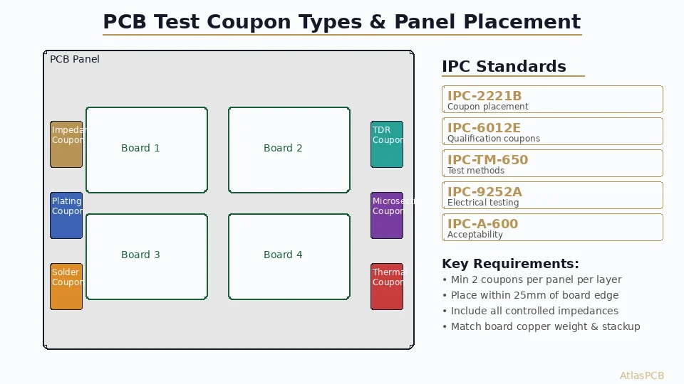
Types of PCB Test Coupons
1. Impedance Test Coupons
The most common coupon type for signal-integrity-critical boards. These replicate the exact trace geometries, dielectric thicknesses, and reference planes from your production design.
Key design rules:
- Include every unique impedance structure (microstrip, stripline, differential pairs)
- Trace lengths: minimum 150mm (6”) for TDR measurement accuracy
- Include calibration structures (THRU, OPEN, SHORT) for de-embedding
- Match copper weight and surface finish to production board
Per IPC-TM-650 Method 2.5.5.7, impedance coupons must be tested using Time Domain Reflectometry (TDR) with a calibrated vector network analyzer. Typical tolerance for production is ±10% of target impedance.
2. Plating Verification Coupons
These coupons verify copper plating thickness uniformity across the panel, particularly critical for:
- Via barrel plating (minimum 25μm per IPC-6012E Class 3)
- Surface copper uniformity
- [Electroless copper]/blog/pcb-electroless-copper-plating-process/) seed layer coverage
Design requirements:
- Include vias matching the highest aspect ratio in your design
- Position coupons at both panel center and edge to capture plating variation
- Include blind/buried vias if present in the production design
3. Microsection (Cross-Section) Coupons
Microsection coupons are designed specifically for destructive cross-sectional analysis. After cutting, mounting, polishing, and etching, they reveal:
- Layer-to-layer registration accuracy
- Drill quality (nail-heading, rough bores)
- [Resin plug quality]/blog/pcb-resin-plug-via-process/) in filled vias
- Dielectric thickness between layers
- Copper distribution and plating voids
4. Thermal Stress Coupons (Solder Float)
These coupons undergo thermal shock testing per IPC-TM-650 Method 2.6.8:
- Float on molten solder at 288°C for 10 seconds (lead-free: 260°C for 20 seconds)
- Examine for delamination, measling, or barrel cracking
- Required for all Class 3 boards and recommended for Class 2
5. Peel Strength Coupons
Designed to measure copper-to-laminate adhesion force (measured in lb/in or N/mm):
- 1” wide copper strip for standard peel test
- Minimum 6 lb/in (1.05 N/mm) for IPC Class 2 inner layers
- Critical for [high-Tg laminates]/blog/pcb-stackup-design-guide/) and alternative surface finishes
6. Solderable Test Coupons
Verify that the board’s surface finish maintains acceptable solderability:
- Wetting balance test per J-STD-003
- Steam aging simulation (8 hours at 93°C, 95% RH)
- Critical for [ENIG]/blog/enig-surface-finish-process/) and other surface finishes with shelf-life concerns
IPC Standards Governing Test Coupons
| Standard | Coverage | Key Requirements |
|---|---|---|
| IPC-2221B | General coupon design | Placement, minimum sizes, feature requirements |
| IPC-6012E | Rigid board qualification | Mandatory coupon types per class, sampling plans |
| IPC-6013D | Flex/rigid-flex boards | Additional flex-specific coupons |
| IPC-TM-650 | Test methods | Specific procedures for each coupon test |
| IPC-9252A | Electrical testing | In-circuit and functional test requirements |
| IPC-A-600 | Visual acceptability | Microsection acceptance criteria |
IPC-6012E Requirements by Class
Class 1 (General Electronics):
- Coupons required for initial qualification only
- Reduced sampling acceptable after process validation
Class 2 (Dedicated Service):
- Impedance coupons on every controlled-impedance panel
- Plating coupons per lot or shift
- Microsection coupons per lot
Class 3 (High Reliability):
- All coupon types required on every production panel
- Thermal stress testing mandatory
- Traceability back to specific panel position required
🔧 Need IPC-Qualified PCBs with Full Coupon Documentation?
AtlasPCB provides comprehensive test coupon design and reporting for Class 2 and Class 3 boards. Every controlled-impedance order includes TDR reports with coupon data. DFM review included with every order.
Get Your Free DFM Review →Test Coupon Design Best Practices
Panel Placement Strategy
The location of coupons on the panel directly impacts measurement accuracy:
- Panel rail placement: Position coupons in the 10-15mm border area (panel rail) that gets routed away after fabrication
- Edge proximity: Keep within 25mm of the outermost board—this zone shares plating current density with production boards
- Avoid corners: Panel corners experience 10-15% higher plating thickness due to current crowding
- Orient along travel direction: For impedance coupons, align traces parallel to the direction the panel travels through the plating line
Impedance Coupon Design Rules
For [controlled-impedance boards]/blog/controlled-impedance-pcb-design-stackup-calculations/):
Minimum trace length:    150mm (6") for TDR accuracy
Trace width:             Match production geometry exactly
Reference plane:         Continuous, unbroken ground
Pad spacing:             SMA launch pads at coupon ends
Differential pairs:      Include both coupled and uncoupled sections
Critical detail: The coupon stackup must exactly replicate the production board. If your board has a buried via between layers 3-6, the coupon must include the same drill and fill sequence—it affects dielectric thickness.
Designing for Microsection Analysis
Microsection coupons require specific features for cross-sectional examination:
- Alignment targets: Include fiducials for precise cut location
- Multiple via sizes: Include your smallest and largest drills
- Layer identification: Add text on each copper layer for registration measurement
- Redundancy: Design at least 3 cut locations per coupon (for multiple samples)
Via Reliability Coupon Design
For [high-reliability via structures]/blog/pcb-via-reliability-testing/):
- Include representative via stacks (through, blind, buried, stacked microvias)
- Design daisy-chain patterns for 4-wire resistance measurement
- Include thermal cycling provisions (IST—Interconnect Stress Testing patterns)
- Match aspect ratios exactly to production design
Common Test Coupon Design Mistakes
Mistake 1: Non-Representative Geometry
Coupons with trace widths or spacing different from the production board give misleading impedance data. Every impedance structure in your design must have a corresponding coupon trace.
Mistake 2: Missing Reference Plane Replication
If your board has split planes, polygon pours, or antipad clearances near impedance traces, the coupon must replicate these conditions.
Mistake 3: Insufficient Trace Length
Short coupon traces (under 100mm) produce TDR measurements dominated by launch-pad discontinuities rather than characteristic impedance. Always exceed 150mm.
Mistake 4: Wrong Position on Panel
Coupons placed in panel centers experience different plating conditions than boards at panel edges. Match position to production board location.
Mistake 5: Single Coupon for Multiple Impedances
Each unique impedance value (50Ω single-ended, 90Ω differential, 100Ω differential) requires its own dedicated coupon trace. Combined coupons with multiple trace widths risk cross-coupling.
Test Coupon Reporting
What Your Fab Should Provide
For a complete quality package, expect these deliverables:
- TDR impedance report: Measured impedance vs. target for each controlled structure
- Microsection photos: Cross-sections at ≥100x magnification showing layer registration, plating quality, and dielectric thickness
- Plating data: Copper thickness measurements at surface and via barrel
- Thermal stress results: Pass/fail after solder float per IPC-TM-650
- Traceability: Panel serial number linking coupons to specific production boards
Reading a TDR Report
A Time Domain Reflectometry report shows impedance as a function of position along the coupon trace:
- Flat profile = consistent impedance (ideal)
- Rising slope = trace narrows or dielectric thins along length
- Spikes at ends = normal launch-pad discontinuities (ignored in measurement)
- Out-of-spec zone = process issue at that panel position
When to Specify Custom Coupons
Standard coupons from your fabricator cover most cases. Specify custom coupons when:
- Your design has unusual stackups (hybrid materials, embedded components)
- You need insertion-loss verification (not just impedance)
- RF applications require phase-matched testing
- Military/aerospace programs demand program-specific coupon sets (AS9100)
- [High-speed SerDes]/blog/differential-pair-routing-rules-high-speed-serdes-pcb/) channels require frequency-domain characterization
Integration with PCB Testing Methods
Test coupons complement—but don’t replace—other [PCB testing methods]/blog/pcb-testing-methods/):
| Method | What It Verifies | Coupon Role |
|---|---|---|
| Flying probe | Net connectivity | Coupons verify plating enabling connectivity |
| TDR testing | Impedance | Coupons are the measurement vehicle |
| [AOI/SPI]/blog/aoi-spi-inspection-pcb-assembly-quality-control/) | Visual defects | Coupons verify underlying material quality |
| ICT fixture | Component values | Coupons ensure pad metallurgy for probing |
| IST | Via reliability | Coupons provide daisy-chain access |
Coupon Data Interpretation
Impedance Measurement Interpretation
When reviewing TDR reports from your fabricator:
- ±5% of target: Excellent process control—suitable for high-speed designs above 10 Gbps
- ±8% of target: Acceptable for most commercial applications (IPC default tolerance)
- ±10% of target: Marginal—investigate whether dielectric thickness or trace width deviates
- >10% deviation: Reject—request root cause analysis and replacement panels
Common causes of impedance deviation:
- Resin content variation in prepreg (affects Dk by 0.1-0.3)
- Etch undercut varying trace width by ±12μm
- Press cycle temperature affecting final dielectric thickness
- Copper foil roughness (RTF vs. VLP) changing effective Dk
Microsection Acceptance Criteria
Per [IPC-A-600]/blog/ipc-a-600-pcb-acceptability-inspection-guide/) acceptability standards:
| Feature | Class 2 Acceptance | Class 3 Acceptance |
|---|---|---|
| Minimum barrel plating | 20μm average | 25μm minimum point |
| Via void (barrel) | ≤2 voids, each <90° arc | No voids permitted |
| Layer registration | ±75μm | ±50μm |
| Dielectric spacing | ≥75μm (after etch) | ≥100μm (after etch) |
| Resin recession | ≤80μm depth | ≤25μm depth |
| Nail-heading | ≤50% of trace width | ≤25% of trace width |
Thermal Stress Test Pass/Fail
After solder float testing per IPC-TM-650 2.6.8:
- Pass: No delamination, blistering, measling, or barrel cracking at 20x magnification
- Marginal: Slight crazing visible—acceptable for Class 2, reject for Class 3
- Fail: Any delamination, barrel crack, or lifted land—reject all affected panels
Cost Considerations
Standard Coupon Package (Included)
Most fabricators include basic coupons at no additional charge:
- 1 impedance coupon per unique stackup per panel
- Process monitoring coupons (plating, registration) per production lot
- Visual inspection coupons as needed
Enhanced Coupon Package ($50-200 per design)
For high-reliability or complex designs:
- Multiple impedance coupons per panel (different frequencies or structures)
- IST (Interconnect Stress Testing) pattern coupons
- Insertion loss (S-parameter) coupons with SMA launch
- Custom microsection targets
Full Qualification Package ($500-2000 per design)
For aerospace, military, or automotive programs:
- Complete IPC-6012E qualification coupon set
- Statistical process control (SPC) data from coupon measurements
- First Article Inspection Report (FAIR) with all coupon data
- Ongoing conformance testing documentation
Conclusion
Test coupon design is a critical but often overlooked aspect of PCB engineering. Properly designed coupons per IPC-2221B and IPC-6012E give you objective, traceable evidence that your board was manufactured correctly—before it ever reaches assembly.
For controlled-impedance designs, specify exact coupon geometries in your fabrication notes. For Class 3 reliability, ensure your fabricator provides panel-level traceability linking coupon data to your specific boards.
Further Reading
- [PCB Impedance Coupon Testing]/blog/pcb-impedance-coupon-testing/) — Deep dive into TDR measurement methodology
- [IPC Standards & PCB Classes Explained]/blog/ipc-standards-pcb-classes/) — Understanding Class 1/2/3 requirements
- [PCB Via Reliability Testing]/blog/pcb-via-reliability-testing/) — IST and thermal cycling verification
- [Controlled Impedance PCB Design]/blog/controlled-impedance-pcb-design-stackup-calculations/) — Stackup calculations and design rules
About AtlasPCB — We specialize in complex PCB manufacturing for HDI, RF, and high-reliability applications. Explore our impedance-controlled PCB manufacturing, or get an full PCB manufacturing capabilities . Every order includes free engineering review. Get your quote.
Reviewed by AtlasPCB Engineering Team — IPC-certified manufacturing specialists with 15+ years of production experience in HDI, RF, and high-reliability PCB fabrication. Content based on factory floor data and real customer design reviews.
- test-coupon
- ipc-standards
- quality-control
- impedance-testing
- pcb-fabrication