· AtlasPCB Engineering · Engineering · 7 min read
PCB Copper Foil Thickness Selection: Inner Layer vs Outer Layer Design Rules
Master copper foil thickness selection for multilayer PCBs. Compare standard 1oz vs heavy 2oz+ copper, understand inner layer vs outer layer considerations, calculate current capacity, and optimize stackup design for impedance control and thermal management.
Understanding PCB Copper Foil: Thickness, Weight, and Selection Criteria
Copper foil thickness is one of the most consequential decisions in PCB stackup design. It directly affects current-carrying capacity, impedance values, thermal dissipation, manufacturing yield, and ultimately product reliability. Yet many designers default to “1oz everywhere” without understanding the trade-offs between inner layer and outer layer copper selection.
This guide provides engineering-level detail on copper foil selection, covering the relationship between thickness and electrical performance, thermal management implications, and manufacturing constraints that shape real-world design choices.
Copper Weight Nomenclature: oz/ft² to Microns
The PCB industry measures copper thickness by “weight” — the mass of copper deposited per square foot of surface area. This convention dates to electroplating processes where copper was measured by weight rather than caliper measurement.
| Copper Weight | Nominal Thickness | Typical Application |
|---|---|---|
| 0.25 oz (H/H oz) | 8.75 µm (0.34 mil) | Ultra-fine HDI inner layers |
| 0.5 oz | 17.5 µm (0.69 mil) | Standard inner layers |
| 1 oz | 35 µm (1.38 mil) | Standard outer layers |
| 2 oz | 70 µm (2.76 mil) | Power/ground planes |
| 3 oz | 105 µm (4.13 mil) | High-current applications |
| 4-6 oz | 140-210 µm | Heavy copper power boards |
Important distinction: The “starting copper” (base foil laminated during layup) differs from “finished copper” (after plating). Outer layers receive an additional 20-30µm of electroplated copper during the through-hole plating process. A board specified as “1oz outer” actually finishes at approximately 55-65µm total copper thickness on outer layers.
Inner Layer vs Outer Layer: Why They Differ
Outer Layer Considerations
Outer layers serve multiple functions simultaneously:
- Component attachment: Solder pads require sufficient copper for reliable joints
- Power distribution: Wide traces or planes carry supply currents
- Signal routing: Controlled-impedance traces for high-speed interfaces
- Environmental protection: Copper under solder mask provides corrosion resistance
The additional plating copper (from through-hole metallization) means outer layers are always thicker than their starting foil weight suggests. A 1oz starting foil finishes at approximately 1.7-2.0oz effective thickness.
Inner Layer Considerations
Inner layers face different constraints:
- Etch resolution: Thicker copper requires wider etch compensation, limiting minimum trace width
- Lamination pressure: Thick inner copper creates resin-starvation risks around traces
- Z-axis dimension: Each additional µm of copper adds to total board thickness
- Impedance uniformity: Thinner, more uniform foil produces more consistent impedance
For a 0.5oz inner layer, minimum trace/space can achieve 3/3 mil (75/75 µm). At 1oz inner, this relaxes to 3.5/3.5 mil. At 2oz inner, expect 5/5 mil minimum — significantly limiting routing density for BGA escape patterns.
Current Capacity Calculations
The IPC-2152 standard provides the most accurate current capacity data for PCB traces. Key variables include:
- Copper cross-sectional area (width × thickness)
- Allowable temperature rise (typically 10°C, 20°C, or 30°C)
- Ambient temperature and airflow conditions
- Internal vs external layer (external traces dissipate heat more efficiently)
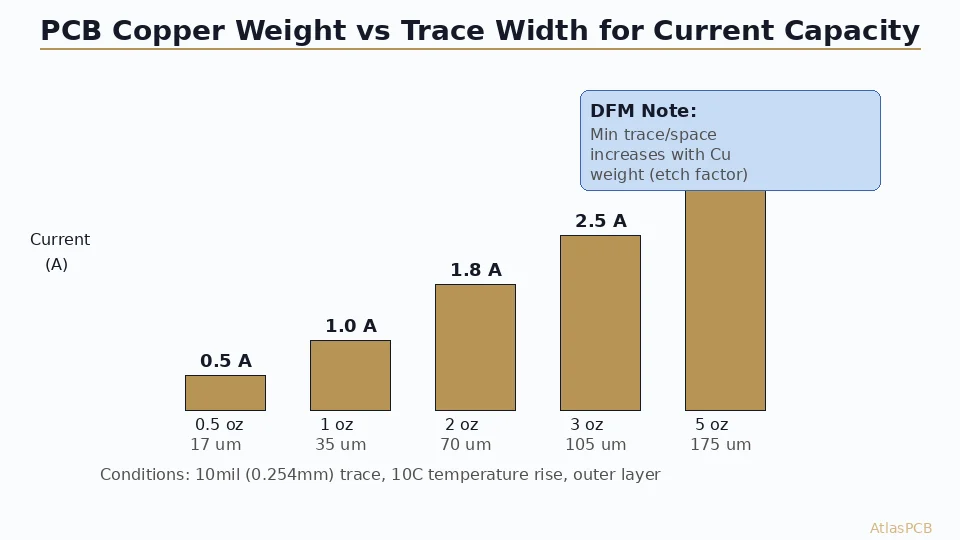
Rule of Thumb for External Traces (20°C Rise)
| Trace Width | 0.5 oz | 1 oz | 2 oz | 3 oz |
|---|---|---|---|---|
| 10 mil | 0.5 A | 1.0 A | 1.6 A | 2.1 A |
| 20 mil | 0.9 A | 1.6 A | 2.8 A | 3.8 A |
| 50 mil | 1.8 A | 3.2 A | 5.5 A | 7.5 A |
| 100 mil | 3.0 A | 5.5 A | 9.5 A | 13 A |
Internal traces carry approximately 50% less current than external traces of the same dimensions, due to reduced convective heat dissipation.
Need Heavy Copper or Controlled-Impedance PCBs?
AtlasPCB manufactures boards from 0.5oz to 6oz copper with ±8% impedance tolerance. Upload your stackup and get a DFM review within 24 hours.
Get Your Stackup Reviewed →Impedance Impact: Copper Thickness in Stackup Calculations
Copper thickness directly enters the impedance equation for both microstrip and stripline configurations. The relationship is not linear — trace thickness affects both the capacitance to reference planes and the inductance of the conductor.
Microstrip (Outer Layer)
For a 50Ω single-ended microstrip on FR-4 (Dk=4.2):
- 1oz copper (35µm finish ~55µm): Trace width ≈ 4.5 mil over 4 mil dielectric
- 2oz copper (70µm finish ~90µm): Trace width ≈ 3.8 mil over 4 mil dielectric
The thicker conductor acts as a wider effective cross-section, pulling impedance lower. Manufacturers compensate by narrowing the trace — but this can conflict with minimum etch requirements.
Stripline (Inner Layer)
For a 50Ω stripline between two reference planes:
- 0.5oz copper (17.5µm): Trace width ≈ 4.2 mil in 8 mil total dielectric
- 1oz copper (35µm): Trace width ≈ 3.5 mil in 8 mil total dielectric
Inner layers benefit from thinner copper because it allows wider traces (easier to manufacture) for the same impedance target. This is one reason 0.5oz inner layers are preferred for impedance-controlled signal routing.
Manufacturing Constraints by Copper Weight
Etch Factor and Minimum Feature Size
Copper etching is never perfectly anisotropic. The “etch factor” describes lateral undercut relative to vertical depth:
| Starting Copper | Etch Factor | Min Trace (mil) | Min Space (mil) |
|---|---|---|---|
| 0.25 oz | 1:1 | 2.0 | 2.0 |
| 0.5 oz | 1:1 | 3.0 | 3.0 |
| 1 oz | 1:0.8 | 3.5 | 3.5 |
| 2 oz | 1:0.7 | 5.0 | 5.0 |
| 3 oz | 1:0.6 | 8.0 | 8.0 |
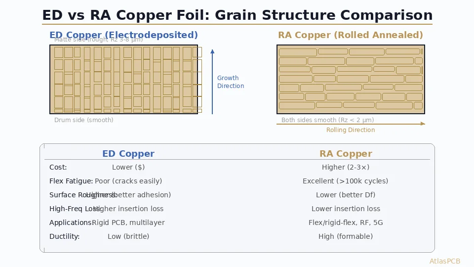
Pattern plating (used for outer layers) achieves better etch factors than panel plating because less copper needs removal. This is why outer layers can maintain finer features despite having heavier total copper.
Lamination and Resin Fill
Thick inner-layer copper creates “valleys” between traces that must be filled with resin during lamination. Insufficient resin fill causes:
- Voids between traces (reliability failure)
- Dielectric thickness variation (impedance instability)
- Delamination under thermal stress
For 2oz+ inner copper, specify high-flow prepreg (>65% resin content) and increased lamination pressure. Some fabricators require “copper-filled” (no large copper-free areas) to ensure uniform pressure distribution.
Thermal Design Optimization
Copper as Heat Spreader
Copper’s thermal conductivity (385 W/m·K) makes it an excellent lateral heat spreader within the PCB. Design strategies include:
- Dedicated thermal planes: Full copper planes on inner layers beneath hot components
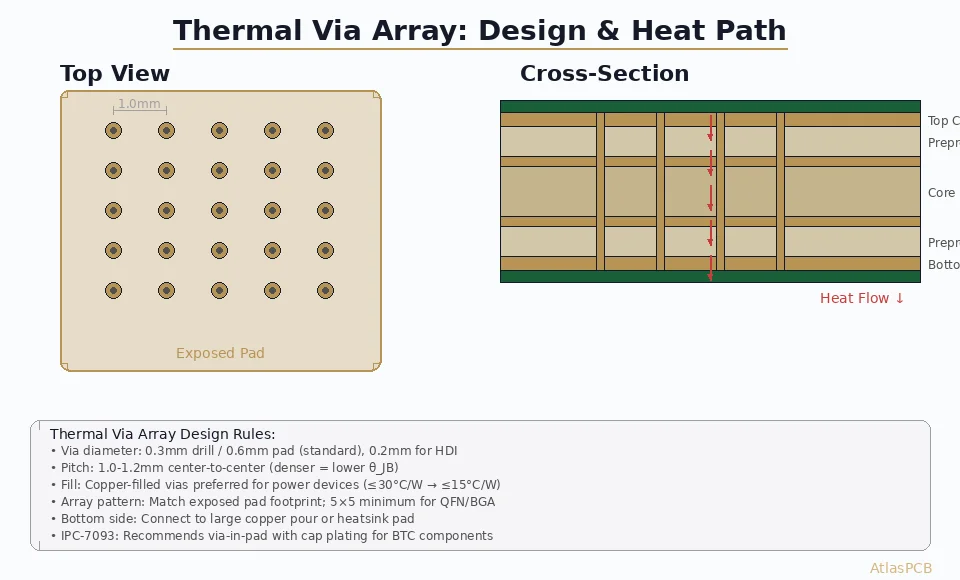
- Thermal via arrays: Connecting component pads to internal copper planes
- Heavy copper on power layers: 2-3oz planes reduce thermal resistance for power delivery
- Hybrid stackups: Mix 2oz power planes with 0.5oz signal layers
Calculating Thermal Resistance
For a copper plane acting as a heat spreader:
R_thermal = t / (k × A)Where:
- t = dielectric thickness above the plane
- k = dielectric thermal conductivity (~0.3 W/m·K for FR-4)
- A = spreading area
A 2oz copper plane (70µm) has negligible thermal resistance itself; the bottleneck is always the FR-4 dielectric between the heat source and the copper plane.
Stackup Design Strategies
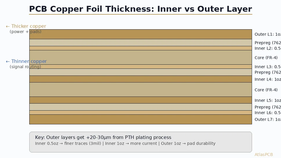
Standard 4-Layer (Cost-Optimized)
L1 (Signal+Power): 1oz start → ~1.7oz finish
Prepreg: 7628, 7.8 mil
L2 (Ground): 0.5oz
Core: 39.4 mil
L3 (Power): 0.5oz
Prepreg: 7628, 7.8 mil
L4 (Signal+Power): 1oz start → ~1.7oz finish
High-Current 6-Layer (Power Electronics)
L1 (Power bus): 2oz start → ~2.7oz finish
Prepreg: 2116×2, 8 mil
L2 (Ground): 1oz
Core: 10 mil
L3 (Signal): 0.5oz
Core: 20 mil
L4 (Signal): 0.5oz
Core: 10 mil
L5 (Ground): 1oz
Prepreg: 2116×2, 8 mil
L6 (Power bus): 2oz start → ~2.7oz finish
HDI 8-Layer (Fine-Pitch BGA)
L1 (Signal): 0.5oz start → ~1.2oz finish
µvia dielectric: 3 mil
L2 (Signal): 0.5oz
Prepreg: 1080, 3 mil
L3 (Ground): 0.5oz
Core: 8 mil
L4 (Signal): 0.5oz
Core: 8 mil
L5 (Signal): 0.5oz
Core: 8 mil
L6 (Ground): 0.5oz
Prepreg: 1080, 3 mil
L7 (Signal): 0.5oz
µvia dielectric: 3 mil
L8 (Signal): 0.5oz start → ~1.2oz finish
Design Decision Flowchart
- Define current requirements: Calculate max current per net
- Set impedance targets: Determine trace widths needed
- Check routing density: Verify BGA escape at chosen copper weight
- Validate thermal needs: Ensure adequate heat spreading
- Confirm manufacturing: Check against fab capabilities
- Iterate stackup: Balance all constraints
Common Mistakes to Avoid
Mistake 1: Specifying heavy copper on signal layers. Using 2oz for signal layers forces wider traces, which wastes routing real estate. Keep signal layers at 0.5oz and route power on dedicated heavy-copper planes.
Mistake 2: Ignoring plating addition on outer layers. Designers who calculate impedance using “1oz” thickness but forget the 20-30µm plating addition get consistently low impedance measurements at fab. Always use “finished copper” in calculations.
Mistake 3: Mixed copper weights without prepreg adjustment. Combining 2oz and 0.5oz inner layers creates step changes that standard prepreg cannot fill uniformly. Specify high-flow prepreg or add copper balancing patterns.
Mistake 4: Underestimating inner-layer current derating. Internal traces carry only ~50% the current of external traces. Designers accustomed to external-layer current tables often under-size inner-layer power traces.
Further Reading
- Controlled Impedance PCB Stackup Design Rules
- PCB Copper Plating Uniformity and Throwing Power
- 16-Layer PCB Stackup Design Guide
- PCB Thermal Via Array Design Rules
Need help selecting the right copper thickness for your stackup? AtlasPCB’s engineering team reviews every order for optimal copper weight selection, impedance accuracy, and manufacturability. Request a free DFM review →
About AtlasPCB — We specialize in complex PCB manufacturing for HDI, RF, and high-reliability applications. Explore our impedance-controlled PCB manufacturing . Every order includes free engineering review. Get your quote.
Reviewed by AtlasPCB Engineering Team — IPC-certified manufacturing specialists with 15+ years of production experience in HDI, RF, and high-reliability PCB fabrication. Content based on factory floor data and real customer design reviews.
- pcb design
- copper thickness
- stackup design
- current capacity
- impedance control
- manufacturing