· AtlasPCB Engineering · Engineering · 11 min read
PCB Copper Plating Process: Electroless vs Electrolytic Copper for HDI Vias and High-Density Interconnects
Compare electroless and electrolytic copper plating processes for HDI PCB manufacturing. Learn desmear preparation, plating chemistry, via fill techniques, and quality metrics that determine microvia reliability in advanced multilayer boards.

Introduction: The Foundation of Every PCB Connection
Every signal trace, power plane, and via connection in a printed circuit board relies on copper plating. Yet the copper plating process remains one of the least understood aspects of PCB manufacturing among designers—even though plating quality directly determines via reliability, impedance consistency, and long-term product life.
For HDI PCBs with microvias, the plating challenge intensifies dramatically. Laser-drilled blind vias with 75-100μm diameters and aspect ratios approaching 1:1 demand precise plating chemistry to achieve void-free copper fill. A single void in a critical via can cause intermittent failures that escape production testing but manifest in field service.
This guide examines both electroless and electrolytic copper plating in detail—the chemistry, process parameters, quality metrics, and manufacturing considerations that determine whether your HDI design achieves production-grade reliability or becomes a yield nightmare.
The Two-Stage Plating Architecture
PCB copper plating is fundamentally a two-stage process, each stage solving a different problem:
Stage 1: Electroless Copper (The Seed Layer)
Problem solved: After drilling, via walls are exposed epoxy resin and glass fiber—both non-conductive. Electrolytic plating requires a conductive surface to deposit onto.
Solution: Chemical (autocatalytic) copper reduction deposits a thin conductive layer without external current.
Stage 2: Electrolytic Copper (The Bulk Conductor)
Problem solved: The electroless layer is too thin (0.3-1.5μm) for current-carrying capacity or mechanical reliability.
Solution: Electrochemical deposition using external current builds copper to final thickness (15-25μm panel plate, or full via fill).
This architecture means electroless plating quality directly constrains electrolytic plating success. No amount of electrolytic optimization can compensate for poor electroless coverage.
Desmear: The Critical Pre-Plating Step
Before any copper touches the via wall, desmear must prepare the surface. This step is frequently underestimated yet accounts for a significant portion of plating-related defects.
Why Desmear Matters
Laser and mechanical drilling generate heat that softens resin, creating a thin “smear” layer coating the via wall. This smear:
- Blocks electrical contact between plated copper and inner layer pads
- Prevents electroless copper adhesion to the dielectric
- Creates delamination initiation sites under thermal stress
The Three-Step Desmear Process
Step 1 — Solvent Swell (Conditioning)
- Chemistry: Glycol ether or N-methyl pyrrolidone (NMP) based
- Temperature: 65-80°C
- Time: 3-5 minutes
- Purpose: Penetrates and swells the resin smear for easier oxidation
Step 2 — Permanganate Etch (Oxidation)
- Chemistry: Potassium permanganate (KMnO₄) 55-80 g/L in caustic solution
- Temperature: 75-85°C
- Time: 5-15 minutes (varies by material system)
- Purpose: Oxidizes and dissolves resin smear, creates micro-roughened surface
- Critical parameter: Etch depth 1-3μm for optimal adhesion
Step 3 — Neutralization (Reduction)
- Chemistry: Acidic solution with reducing agent (hydroxylamine or peroxide)
- Temperature: 40-50°C
- Time: 3-5 minutes
- Purpose: Removes MnO₂ residue that would inhibit plating catalysis
Desmear Quality Metrics
| Parameter | Acceptable Range | Risk if Out of Spec |
|---|---|---|
| Etch depth | 1-3 μm | Under: poor adhesion; Over: glass fiber exposure |
| Surface roughness (Ra) | 0.3-1.0 μm | Under: peel failure; Over: plating thickness variation |
| Residual MnO₂ | None visible | Inhibits Pd catalyst, creates voids |
| Glass fiber exposure | <25% protrusion | Wicking, CAF growth, reliability failure |
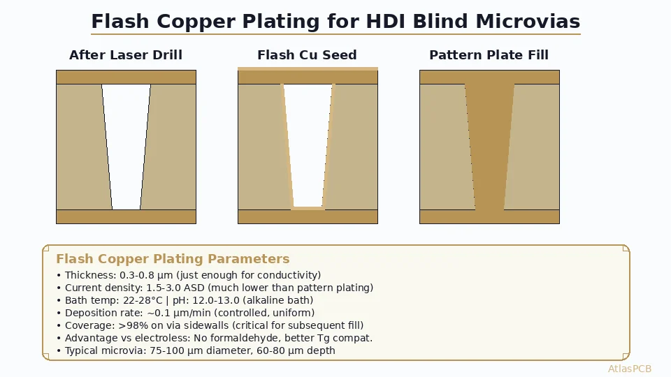
Electroless Copper Plating In Depth
Chemistry Overview
Electroless copper uses formaldehyde as the reducing agent in an alkaline solution:
Cu²⁺ + 2HCHO + 4OH⁻ → Cu⁰ + 2HCOO⁻ + 2H₂O + H₂↑The reaction is catalyzed by palladium (Pd) nuclei deposited in a preceding activation step.
Process Sequence
1. Cleaner/Conditioner (2-5 min, 45-55°C)
- Removes organic contaminants
- Conditions surface for uniform catalyst adsorption
- Surfactant-based, mildly alkaline
2. Micro-Etch (1-3 min, 25-35°C)
- Roughens existing copper surfaces for adhesion
- Typically sodium persulfate or sulfuric acid/peroxide
- Target: 1-2 μm copper removal
3. Pre-Dip/Catalyst (3-5 min, 25-40°C)
- Palladium-tin colloidal catalyst (Pd/Sn)
- Adsorbs onto conditioned surfaces
- Provides nucleation sites for copper deposition
- Alternative: ionic Pd systems for finer control
4. Accelerator (2-4 min, 25-35°C)
- Removes tin from Pd/Sn colloid, exposing active Pd
- Acidic solution activates catalytic surface
- Critical for uniform initiation
5. Electroless Copper Bath (15-30 min, 30-38°C)
- Cu²⁺ source: CuSO₄ (8-12 g/L Cu)
- Reducing agent: HCHO (2-4 g/L)
- Complexant: EDTA or quadrol (30-40 g/L)
- Stabilizer: Various (cyanide-free preferred)
- pH: 12.0-13.0
- Deposition rate: 2-4 μm/hour
Critical Process Parameters
Temperature control: ±1°C is essential. Too hot = bath instability and plate-out; too cold = incomplete coverage.
pH maintenance: Must stay within 12.0-13.0. Below 12: slow deposition, pinholes. Above 13: bath decomposition risk.
Formaldehyde concentration: Consumed during plating, must be replenished. Low HCHO = incomplete coverage in deep vias.
Copper-to-HCHO ratio: Imbalanced ratios cause rough deposits or hydrogen pitting.
Air injection: Controlled agitation ensures fresh chemistry reaches deep via interiors. Over-agitation oxidizes HCHO.
Electroless Copper Quality Indicators
- Coverage: 100% of via walls, no bare spots (verified by backlight test)
- Thickness: 0.5-1.5 μm (measured by cross-section or XRF)
- Adhesion: >0.5 N/mm peel strength to dielectric
- Uniformity: <30% thickness variation board-to-board
- Surface morphology: Fine-grained, no nodules or roughness spikes
Electrolytic Copper Plating In Depth
Panel Plating vs Pattern Plating
Two fundamental approaches exist:
Panel plating (most HDI processes):
- Plate entire panel with copper (15-20 μm)
- Apply photoresist and image circuit pattern
- Etch away unwanted copper
- Advantage: Uniform copper in vias, better impedance control
- Disadvantage: More copper to etch, higher waste
Pattern plating (traditional processes):
- Apply photoresist and image pattern first
- Plate copper only where needed (20-30 μm)
- Strip resist, flash-etch base copper
- Advantage: Less copper waste, thicker traces possible
- Disadvantage: Non-uniform via plating, “dog-bone” effect
DC Plating Chemistry
Basic acid copper sulfate bath:
- CuSO₄·5H₂O: 200-250 g/L
- H₂SO₄: 50-80 g/L
- Chloride (Cl⁻): 40-80 ppm
- Temperature: 22-28°C
- Current density: 1.5-3.0 A/dm² (ASD)
- Agitation: Continuous solution movement + air
Organic additives (critical for throwing power and fill):
- Suppressor (polyethylene glycol): Inhibits plating on exposed surfaces
- Accelerator (bis-3-sulfopropyl disulfide, SPS): Promotes plating in confined areas
- Leveler (Janus Green B or proprietary): Reduces surface bumps, improves uniformity
The interplay of these three additives determines whether copper plates uniformly across the panel or preferentially fills vias.
Pulse-Reverse Plating for Via Fill
Standard DC plating deposits copper uniformly on all surfaces. For blind via fill, this creates a problem: the via opening closes before the bottom fills, trapping a void.
Pulse-reverse (PR) plating solves this:
Forward pulse: 5-20 ms at 3-8 ASD (deposits copper)
Reverse pulse: 1-5 ms at 2-5 ASD (dissolves surface copper)
Off time: 0-5 ms (ion replenishment)
Why it works: The reverse pulse preferentially removes copper from the via opening (highest current density point) while barely affecting copper deep inside the via (shielded by geometry). This maintains an open mouth while the bottom fills up.
Result: Void-free copper fill in blind vias up to 150μm depth with aspect ratios of 1:1.
Via Fill Quality Metrics
| Metric | Target | Measurement Method |
|---|---|---|
| Dimple depth | <15 μm | Cross-section + profilometry |
| Void content | 0% (Class 3) | Cross-section + X-ray |
| Copper thickness uniformity | ±20% across panel | 4-wire resistance or XRF |
| Surface roughness | <3 μm Rz | Profilometry |
| Filling percentage | >95% | Cross-section image analysis |
Need HDI PCBs with Reliable Via Fill?
AtlasPCB uses pulse-reverse plating with real-time dosing control to achieve void-free microvia fill in vias down to 75μm diameter. Our process supports stacked via configurations up to 4-deep.
Get HDI Quote →Throwing Power and High Aspect Ratio Challenges
What is Throwing Power?
Throwing power describes a plating bath’s ability to deposit copper uniformly across varying geometries—particularly inside deep vias versus on flat panel surfaces.
Ideal throwing power: Equal thickness inside via barrel and on panel surface (ratio = 1:1) Typical DC bath: 0.5-0.7:1 ratio for through-hole vias (thinner inside) Optimized PR bath: 0.9-1.2:1 ratio (can overfill for via plugging)
Aspect Ratio Limitations
As via aspect ratio (depth ÷ diameter) increases, plating challenges multiply:
- <0.5:1: Straightforward DC plating, minimal optimization needed
- 0.5-0.8:1: DC plating possible with optimized additives
- 0.8-1.0:1: Pulse-reverse recommended for void-free fill
- 1.0-1.5:1: Advanced PR recipes required, careful process control
- >1.5:1: Extremely challenging, may require multi-step approaches
Solutions for Deep Vias
For high-aspect-ratio through-holes (mechanical drilling):
- Extended plating time with periodic reverse pulses
- High throwing power additive packages
- Solution agitation optimization (eductors targeting via interiors)
- Temperature profiling during long plating cycles
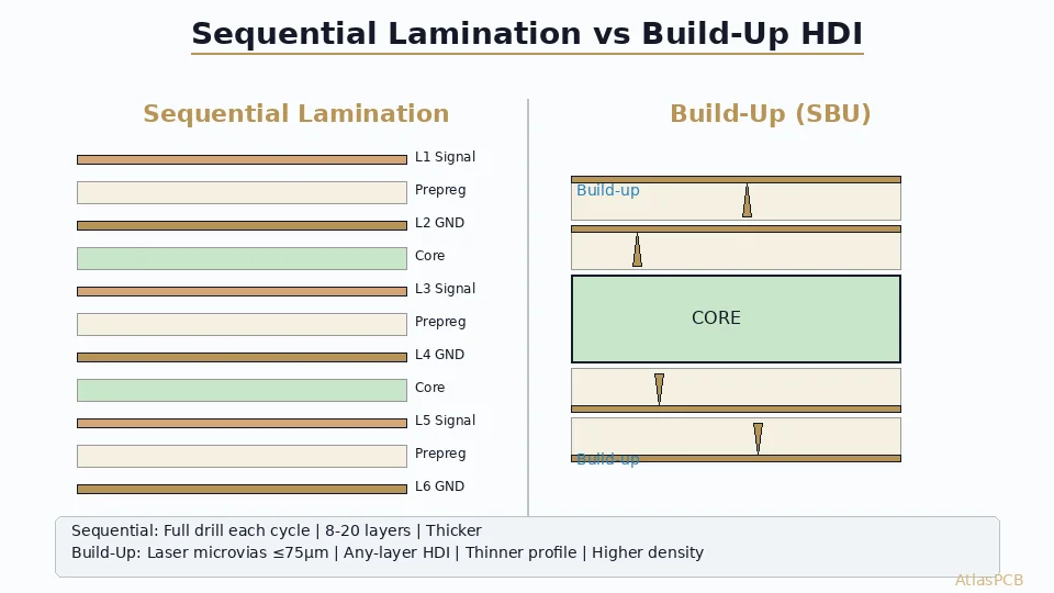
For stacked microvias ([HDI constructions]/blog/hdi-pcb-stackup-design-advanced-en/)):
- Sequential build-up with intermediate planarization
- Each via layer filled and capped before next layer
- Cross-section verification at each build-up stage
- Process window validation per via depth/diameter combination
Process Control and Troubleshooting
Common Plating Defects
Voids in vias:
- Cause: Insufficient throwing power, air entrapment, or contamination
- Solution: Optimize PR parameters, improve wetting, CVS analysis
Nodules (bumps on surface):
- Cause: Particulate contamination or organic breakdown products
- Solution: Carbon treatment, continuous filtration, bath dump/remake
Rough deposit:
- Cause: Low additive concentration or organic contamination
- Solution: CVS dosing adjustment, activated carbon treatment
Thin spots on via walls:
- Cause: Poor electroless coverage, gas bubbles during plating
- Solution: Improve desmear/activation, optimize air agitation
Dog-boning (thick edges, thin center):
- Cause: Current distribution issues in pattern plating
- Solution: Auxiliary anodes, thief patterns, current density reduction
Cyclic Voltammetric Stripping (CVS) Analysis
CVS is the primary tool for monitoring organic additive levels in electrolytic baths:
- Frequency: Every 4-8 hours of production, or per panel batch
- Measures: Suppressor, accelerator, and chloride activity
- Action: Automated dosing systems replenish based on CVS results
- Critical for: Maintaining consistent via fill quality over bath life
Hull Cell Testing
Hull cell panels provide quick assessment of plating bath condition:
- Frequency: Daily or per shift
- Reveals: Current density range performance, brightness, roughness
- Supplements: CVS data with visual deposit quality check
- Training tool: Helps operators recognize bath chemistry shifts
Special Plating Processes for Advanced Applications
Copper-Filled Microvias (POFV)
Plating of Filled Vias (POFV) enables truly planar surfaces for stacking:
- Laser drill blind via
- Desmear and activate
- Electroless copper seed
- Electrolytic via fill (PR plating to overfill)
- Surface planarization (mechanical polishing)
- Panel plate to final thickness
Result: Flat surface suitable for via-on-via stacking without dimple defects.
Direct Metallization (Electroless-Free)
Carbon-based or conductive polymer processes offer electroless alternatives:
- Shadow™ (Macdermid): Graphite-based conductive layer
- BlackHole™ (Macdermid): Carbon black dispersion
- Neoganth™ (Atotech): Conductive polymer
Advantages: No formaldehyde, no Pd catalyst, simpler chemistry Limitations: Higher resistance seed layer, may require slightly higher initial current Application: Standard through-hole PCBs, not recommended for fine-line HDI
Via-in-Pad Plating
[Via-in-pad]/blog/via-in-pad-design/) places vias directly under component pads, requiring:
- Via fill to <15μm dimple
- Mechanical planarization (belt sander or CMP)
- Cap plate (5-10μm additional copper over filled via)
- Final surface finish application
Quality requirements:
- No dimple visible after cap plate
- Planar surface for reliable solder joint formation
- No outgassing from trapped chemistry during reflow
Design Implications for Engineers
DFM Guidelines Related to Plating
When designing HDI PCBs, these plating-related rules affect your layout:
Microvia design:
- Minimum diameter: Dependent on manufacturer capability (50-75μm typical)
- Aspect ratio: Keep ≤1:1 for reliable fill, ≤0.8:1 for Class 3
- Pad size: Minimum 2× via diameter for plating current distribution
- Stacking limit: Verify manufacturer capability (typically 2-3 stacked max)
Through-hole design:
- Minimum annular ring: 75μm (Class 2), 100μm (Class 3) after plating
- Aspect ratio: 10:1 maximum for reliable wall plating
- Thermal relief: Consider for power planes to reduce plating stress
Copper balance:
- Panel copper distribution: <30% variation area-to-area
- Thieving patterns: Add copper in sparse areas for uniform plating
- Trace width compensation: Account for etch factor in final dimensions
How to Specify Plating Requirements
On fabrication drawings, specify:
- Minimum finished copper thickness: Via walls, surface traces
- Via fill requirement: Plugged, filled, or tented
- Dimple specification: Maximum depth after fill/planarization
- Cross-section requirements: Quantity and sampling criteria
Quality Verification Methods
Cross-Section Analysis
The gold standard for plating quality verification:
- Preparation: Epoxy mount, grinding, polishing to mid-via
- Measurements: Wall thickness (minimum, average), void detection
- Magnification: 200-500× for microvia assessment
- Frequency: Per lot or per panel (Class 3)
- Standards: IPC-6012E Table 3-5 for acceptability criteria
Non-Destructive Testing
X-ray inspection:
- Void detection in filled vias without sectioning
- Quick screening of entire panel population
- Limited resolution (~25μm) for smallest defects
4-wire resistance measurement:
- Verifies via chain continuity
- Detects thin plating or cracks
- Production-speed testing possible
TDR (Time Domain Reflectometry):
- Identifies impedance discontinuities from plating variations
- Used for controlled impedance verification
- Requires test coupon integration
Environmental and Safety Considerations
Chemical Management
PCB plating uses hazardous materials requiring proper controls:
- Formaldehyde (electroless): Carcinogen—require ventilation and monitoring
- Sulfuric acid (electrolytic): Corrosive—PPE and containment
- Permanganate (desmear): Oxidizer—storage segregation
- Palladium catalyst: Precious metal—recycling programs
Waste Treatment
Rinse water management:
- Counter-current cascade rinsing reduces water consumption 70%
- Copper recovery from rinse water via ion exchange or electrolysis
- Drag-out reduction through controlled withdrawal speeds
Spent bath disposal:
- Formaldehyde destruction (oxidation or biological treatment)
- Copper recovery from electrolytic baths
- EDTA complexant requiring specialized waste treatment
- Regulatory compliance per local environmental standards
Conclusion: Plating Quality Determines PCB Reliability
The copper plating process—from desmear through electroless seed deposition to electrolytic via fill—represents the most critical manufacturing sequence in HDI PCB fabrication. Every subsequent process (imaging, etching, surface finishing) builds upon the foundation that plating provides.
Key takeaways for PCB designers:
- Aspect ratio drives complexity: Design vias within your manufacturer’s proven capability
- Copper balance matters: Uniform copper distribution enables uniform plating
- Via fill isn’t free: Filled and planarized vias require additional process steps and cost
- Cross-sections tell the truth: Request verification data for critical applications
- DFM consultation prevents surprises: Engage your manufacturer early for challenging designs
Understanding plating fundamentals empowers better design decisions. When you know that a 1:1 aspect ratio microvia requires pulse-reverse chemistry with 20+ minutes of plating time, you can make informed trade-offs between routing density and manufacturing risk.
Ready to discuss your HDI plating requirements? AtlasPCB’s process engineering team specializes in [advanced via fill technology]/blog/hdi-pcb-stackup-design-advanced-en/) for stacked microvia constructions. Get a quote with guaranteed plating quality specifications backed by cross-section verification data.
Further Reading
- [Buried Via Technology in High-Density PCBs: Design Rules, Fabrication & Cost]/blog/pcb-buried-via-technology/)
- [Rogers PCB Fabrication: Material Sourcing, Lead Times & Quality Control]/blog/rogers-pcb-fabrication/)
- [HDI PCB Design for 5G Antenna Integration: Signal Integrity Challenges in Millimeter-Wave Applications]/blog/hdi-5g-antenna-integration-pcb-design/)
- [PCB Via Size Guide: Mechanical, Laser & Microvia Dimensions]/blog/pcb-via-size-selection-guide/)
- [HDI PCB Manufacturer: How to Choose the Right Partner for Complex Boards]/blog/hdi-pcb-manufacturer/)
- Our Manufacturing Capabilities
About AtlasPCB — We specialize in complex PCB manufacturing for HDI, RF, and high-reliability applications. Explore our HDI PCB manufacturing capabilities, free engineering DFM review, or get an full PCB manufacturing capabilities . Every order includes free engineering review. Get your quote.
Reviewed by AtlasPCB Engineering Team — IPC-certified manufacturing specialists with 15+ years of production experience in HDI, RF, and high-reliability PCB fabrication. Content based on factory floor data and real customer design reviews.
- copper plating
- electroless copper
- electrolytic plating
- HDI PCB
- microvia
- PCB manufacturing
- DFM