· AtlasPCB Engineering · Engineering · 9 min read
How to Specify PCB Edge Plating: Fab Drawing Requirements and DFM Rules
Complete specification guide for PCB edge plating (castellated edges, plated board edges). Includes fab note examples, dimensional tolerances, design rules, and common DFM failures to avoid.
Quick Reference: Edge Plating Fab Note Template
Copy this into your fabrication drawing and modify the bracketed values:
EDGE PLATING REQUIREMENTS:
1. Plated board edges as indicated on mechanical drawing layer
2. Minimum copper thickness on plated edges: 25um (1.0mil)
3. Copper wraparound: minimum 0.2mm from edge onto top/bottom surfaces
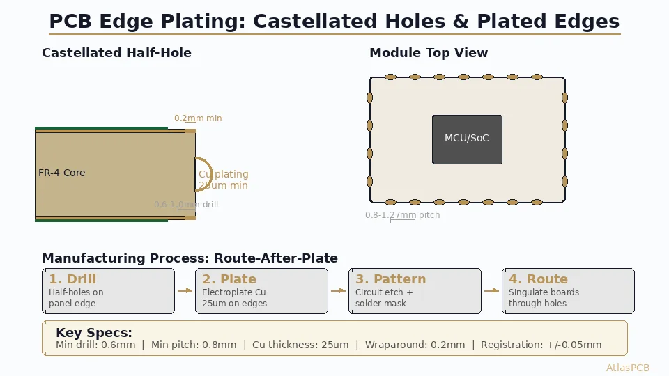
4. Process: Route-after-plate (plating applied before board singulation)
5. Edge locations: [EDGE A - full length] [EDGE B - partial, see dimensions]
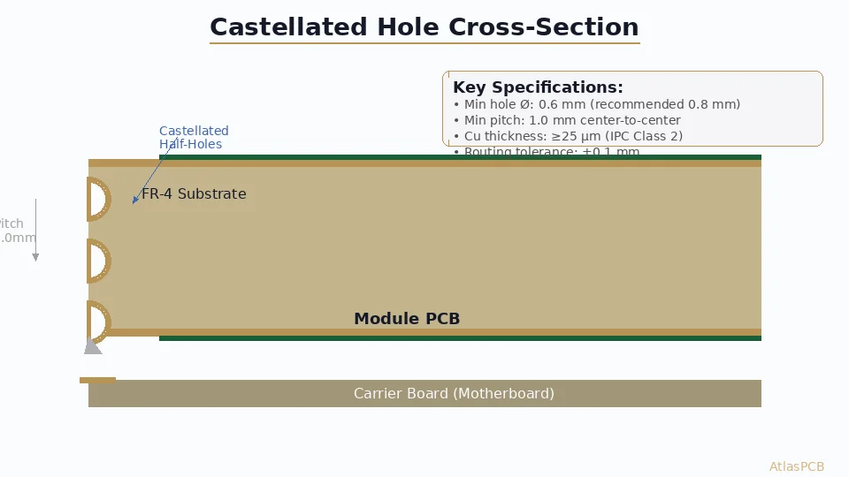
6. Castellated half-holes: [0.8mm drill diameter, 1.0mm pitch]
7. Plated edge surface finish: [same as board surface finish / bare copper]
8. IPC-6012 Class [2/3] acceptance criteriaThis template covers 90% of edge plating specifications. The most commonly missed items are the copper wraparound dimension and the explicit route-after-plate process callout.
Why Edge Plating Specifications Get Rejected
Edge plating is one of the most frequently mis-specified features in PCB fabrication drawings, generating more engineering queries (EQs) per occurrence than almost any other board feature. The core problem is that standard PCB design tools treat the board edge as a simple outline, not as a functional plated surface. This disconnect means designers must communicate edge plating requirements through fab notes, mechanical layers, and drill files that were not designed for this purpose.
The most common rejection reason is ambiguity: a designer places half-holes on the board edge in their drill file, but provides no fab note explaining whether those are intentional castellated features requiring plating or accidental placements. Fabricators who encounter unreferenced half-holes will issue an EQ rather than assuming intent, adding 1-2 days to your lead time. The second most common issue is specifying edge plating without indicating the manufacturing sequence—route-before-plate versus route-after-plate produces dramatically different results, and the fabricator needs explicit direction.
A well-specified edge plating design should add zero engineering queries to your order. The investment in a complete fab note (five minutes of typing) saves days of back-and-forth and prevents costly re-fabrication when assumptions are wrong.
Edge Plating Process: Route-After-Plate vs Route-Before-Plate
The manufacturing sequence determines everything about your edge plating quality, and specifying the wrong sequence is a guaranteed path to delamination or inadequate coverage.
Route-after-plate (standard, recommended): The boards remain in the production panel during all plating steps. Copper is electrodeposited onto the board edges while they are still connected to the panel frame via tabs or remain un-routed. After plating, surface finish, and solder mask, the boards are routed out of the panel along the pre-plated edges. This produces the most reliable edge plating because the copper is deposited under controlled electroplating conditions with uniform current distribution.
The disadvantage of route-after-plate is that it requires careful coordination between the routing program and the plating pattern. The route bit must cut exactly through the center of the plated region, and any misalignment between the plating mask and the routing program creates asymmetric copper on the left versus right halves of the routed edge. Fabricators with tight registration capability (plus/minus 0.05mm) handle this routinely, but it is a genuine manufacturing challenge that not all shops execute well.
Route-before-plate (specialty process): The board edges are routed first, then the exposed edges are plated in a subsequent step. This approach is used when the edge geometry is too complex for route-after-plate (non-linear edges, inside corners, partial-length plating). The disadvantage is that electroplating onto an already-exposed fiberglass edge requires additional surface preparation (plasma or chemical activation of the glass-epoxy interface), and adhesion is inherently lower than copper-to-copper bonding in the route-after-plate method.
For most designs, specify route-after-plate unless your fabricator specifically recommends otherwise.
PRECISION EDGE PLATING
Castellated Holes and Plated Edges
Route-after-plate process with plus/minus 0.05mm registration. Minimum 25um edge copper. IPC Class 2/3 inspection.
Get DFM Review ›Castellated Holes: Design Rules and Dimensional Requirements
Castellated holes are the most common form of edge plating, used primarily for solder-down module connections. When your board will be soldered as a module onto a carrier board, castellated edges provide a visible solder fillet that can be inspected optically—a significant quality advantage over LGA (land grid array) connections that hide solder joints underneath the module.
The critical dimensional relationships for castellated holes are:
Drill diameter: Minimum 0.6mm recommended. This produces a 0.3mm radius semicircle on each half after routing. Smaller drills (0.5mm) are possible but increase the risk of drill breakage at the board edge and produce very small solder pads that are difficult to inspect. For hand-soldering rework, 0.8-1.0mm drill diameter is preferred.
Pitch (center to center): Minimum 0.8mm for 0.6mm drills, with 1.0mm being standard for most module designs. Tighter pitch is possible but requires the fabricator to use smaller route bits between castellations, increasing routing time and cost. At 1.27mm pitch (50mil), castellated designs are straightforward for any capable fabricator.
Pad extension onto board surface: The copper pad on the top and bottom surfaces should extend minimum 0.3mm from the board edge inward. This wraparound pad provides the solder wetting surface and anchors the plated edge to the board copper layers. Insufficient pad extension is the primary cause of castellated pad delamination during thermal cycling.
Edge-to-drill registration: The routing cut must pass through the exact center of each drilled hole. Misregistration shifts more copper to one half of the cut, producing asymmetric castellations. Specify plus/minus 0.05mm maximum misregistration in your fab notes. AtlasPCB achieves plus/minus 0.05mm edge-to-drill registration as standard for castellated hole designs.
Non-plated gaps between castellated holes: If your module design requires grounding castellations alternating with signal castellations, you can specify non-plated gaps by placing the board outline between holes (no drill at that edge segment). Alternatively, use solder mask over specific castellations to block solder wetting while maintaining the structural copper.
RF Shielding Edge Plating: Continuous Perimeter Ground
Beyond castellated module connections, edge plating serves a critical role in RF shielding. A continuous plated edge connecting the top ground pour to the bottom ground pour creates a faraday cage wall without requiring a separate shield can component. This technique is used in multi-module RF assemblies where individual PCB modules need isolation from adjacent stages, and in mixed-signal designs where digital noise must be contained.
For RF edge plating, the copper thickness requirement is driven by skin depth rather than mechanical reliability. At 1 GHz, the skin depth in copper is approximately 2.1um, meaning a 25um plated edge provides 12 skin depths of attenuation—more than adequate for 60+ dB isolation. However, at frequencies below 100 MHz, skin depth exceeds 6.6um, and the continuous edge creates a lower-impedance ground path that reduces emissions from the board edge.
The design rule for RF edge plating is that the plated edge must connect directly to ground planes on every layer of the stackup. Place ground vias within 0.5mm of the board edge at spacing less than lambda/20 at your highest frequency of concern. These vias ensure the edge plating connects to internal ground planes with low inductance, preventing the edge from becoming a resonant slot antenna at specific frequencies.
RF PCB FABRICATION
Edge Plating for EMI Shielding
Continuous perimeter plating, via fencing, and shield can landing pads. Rogers and FR-4 hybrid constructions available.
Common DFM Failures and How to Prevent Them
After reviewing thousands of edge plating designs, the following failure modes account for 80% of production quality issues. Each is preventable with proper specification.
Failure 1: Copper peeling at the board edge. Root cause is almost always contamination of the edge surface before plating, or insufficient mechanical keying of the glass-epoxy substrate. Prevention: specify route-after-plate process (copper deposits on fresh-cut surface immediately), and ensure your board outline does not pass through large copper-free zones where the router exposes bare laminate that resists plating adhesion. If your design has a ground pour on the outer layers, extend it to within 0.1mm of all plated edges to ensure the plating has a copper landing surface.
Failure 2: Thin copper at 90-degree corners. Where the board surface meets the board edge, current density drops during electroplating due to the geometric shadow effect. This creates a thin spot that is the first point of failure during thermal cycling. Prevention: specify minimum corner thickness (typically 15um even when face thickness is 25um), or request that the fabricator add a 0.1-0.2mm radius to the edge-to-surface transition. Some fabricators achieve this naturally through their routing process; others require explicit specification.
Failure 3: Castellated hole burrs. After routing through plated holes, small copper burrs can remain on the cut edge. These burrs can cause shorts between adjacent castellated pads or prevent proper seating of the module during assembly. Prevention: specify burr-free routing (typically requires a finishing pass with a fresh bit) and maximum burr height of 0.05mm in your fab notes. Cross-section inspection of first articles should verify clean cuts.
Failure 4: Solder mask encroaching on plated edges. If solder mask is applied after edge plating but before routing, mask residue on the plated edge prevents solder wetting during module assembly. Prevention: specify solder mask pullback of 0.15mm minimum from the board edge on all surfaces adjacent to plated edges. Some designers prefer to mask the entire edge plating region as NPTH (no solder mask) in their Gerber files.
ATLASPCB
Submit Your Edge Plating Design for DFM Review
Upload Gerber files and receive a detailed manufacturability report covering edge plating registration, copper coverage, and process recommendations.
Get Instant Quote ›Related Reading:
About AtlasPCB — We specialize in complex PCB manufacturing for HDI, RF, and high-reliability applications. Explore our free engineering DFM review . Every order includes free engineering review. Get your quote.
Reviewed by AtlasPCB Engineering Team — IPC-certified manufacturing specialists with 15+ years of production experience in HDI, RF, and high-reliability PCB fabrication. Content based on factory floor data and real customer design reviews.
- PCB edge plating
- castellated holes
- plated edges
- DFM
- fab drawing
- PCB specification