· AtlasPCB Engineering · Engineering · 9 min read
PCB Panelization and Array Design: V-Score vs Tab Routing, DFM Rules, and Cost Optimization
Complete PCB panelization guide covering V-score vs tab routing vs jump scoring, panel size optimization for SMT lines, fiducial placement, tooling strip design, breakaway tab rules, and DFM best practices to maximize yield and minimize assembly cost.

Introduction: Why Panelization Matters
Individual PCBs are small. SMT assembly machines need something to grip. This fundamental mismatch drives panelization—the practice of combining multiple individual PCBs into a larger panel that can be efficiently processed through pick-and-place machines, reflow ovens, wave soldering, and automated test equipment.
Good panelization design directly impacts:
- Assembly cost: More boards per panel = lower cost per board
- Quality: Proper panel design prevents warping, misalignment, and depaneling damage
- Yield: Poor panelization causes board damage, solder joint cracking, and assembly line jams
- Lead time: Non-standard panel sizes may require custom fixtures, adding days to your schedule
Despite its importance, panelization is often an afterthought—engineers focus on circuit design and routing, then scramble to create a panel at the last minute. This guide covers everything you need to design optimized PCB panels from the start. For related assembly topics, see our [solder paste stencil design guide]/blog/pcb-solder-paste-stencil-design/) and [reflow soldering optimization]/blog/reflow-soldering-profile-optimization-lead-free-pcb-assembly/).
Panel Anatomy: Key Components
A well-designed PCB panel includes:
Board Array
The individual PCBs arranged in rows and columns. The array should maximize board count while maintaining adequate support structure.
Tooling Strips (Rails)
Strips of bare board material (5-10mm wide) along two or four edges of the panel. These provide:
- Machine grip area: Conveyor rails in SMT lines grip the tooling strips
- Fiducial markers: Global fiducials for machine vision alignment
- Tooling holes: 2-3 tooling holes (typically 2.0-4.0mm diameter, non-plated) for fixture registration
- Test coupons: Impedance test coupons, cross-section samples, and date codes (for controlled impedance boards—see our [impedance design guide]/blog/controlled-impedance-pcb-design-stackup-calculations/))
- Bad-mark locations: Positions for marking non-functional boards in the array
Separation Features
V-score lines, routed slots with tabs, or a combination. These define where individual boards will be separated after assembly.
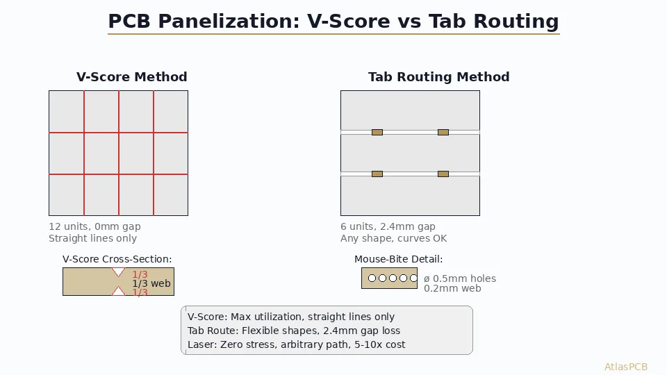
V-Score: When and How
How V-Scoring Works
V-scoring uses a circular blade to cut a V-shaped groove into both the top and bottom surfaces of the panel along straight lines. The groove typically removes 1/3 of the board thickness from each side, leaving 1/3 as a web connecting the boards.
V-Score Profile (1.6mm board):
Top surface
  \_____/     ← V-groove, ~30° angle, 0.5mm deep
  |     |     ← Remaining web, ~0.5mm
  /‾‾‾‾‾\     ← V-groove, ~30° angle, 0.5mm deep
Bottom surface
Separation is performed by a pizza cutter depaneling machine or by hand snapping along the score line.
V-Score Advantages
- Minimal material waste: Score lines consume zero board area (no routing gap)
- Fast processing: Scoring is faster than routing
- Clean edges: When properly scored and separated, edges are clean with minimal dust
- Cost-effective: Lower tooling cost compared to routed panels
V-Score Limitations
- Straight lines only: V-score must run in straight lines across the entire panel width or length. No L-shapes, curves, or partial scores
- Rectangular boards only: Boards must be rectangular to use V-score on all edges
- Edge stress: Separation creates bending stress that can crack solder joints near the score line
- Minimum board thickness: Not recommended for boards thinner than 0.6mm (insufficient remaining web)
- Component clearance: All components and copper features must be ≥1.0mm from score lines
V-Score Design Rules
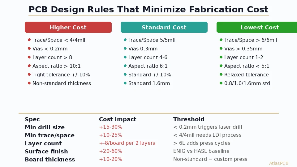
| Parameter | Standard Rule | Tight Rule |
|---|---|---|
| Score depth (per side) | 1/3 of board thickness | Up to 40% |
| Remaining web | 1/3 of board thickness | Minimum 0.4mm |
| Component clearance | ≥1.0mm from score line | ≥1.5mm recommended |
| Trace clearance | ≥0.5mm from score line | ≥1.0mm recommended |
| Copper clearance | ≥0.3mm from score line | ≥0.5mm recommended |
| Score angle | 30° (standard) | 20-45° range |
| Score line tolerance | ±0.1mm | ±0.05mm (precision) |
Tab Routing: When and How
How Tab Routing Works
Tab routing uses a CNC router (typically 2.0mm diameter bit) to cut the board outline, leaving small bridges (tabs) connecting the individual boards to the panel frame or to each other. After assembly, boards are separated by cutting through the tabs using a router depaneling machine, die punch, or manual nippers.
Tab Types
Solid Tabs: Continuous material bridges, typically 1.5-3.0mm wide. Clean but require a depaneling router or die for separation. Best for automated depaneling.
Perforated Tabs (Mouse Bites): Tabs with a row of small drilled holes (0.5mm diameter, 0.8mm pitch) that create a perforated tear line. Can be separated by hand snapping. Leaves a rough edge with small nubs.
Stamp Holes: Larger holes (1.0mm) at wider spacing. Easier to break but rougher edge quality than mouse bites.
Tab Design Rules
| Parameter | Standard Rule | Notes |
|---|---|---|
| Tab width | 1.5-3.0mm | Wider for heavy boards |
| Tab web (solid) | 0.3-0.5mm | Connection point |
| Mouse bite holes | 0.5mm drill, 0.8mm pitch | 5-8 holes per tab |
| Tabs per edge | 2-3 (short), 4-5 (long) | Depends on edge length |
| Tab-to-corner distance | ≥3mm | Prevents corner cracking |
| Routing gap | 2.0-2.4mm | Equals router bit diameter |
| Component clearance | ≥0.5mm from routed edge | Less critical than V-score |
When to Choose Tab Routing Over V-Score
- Board outline is non-rectangular (irregular shapes, internal cutouts, rounded corners)
- Components or traces are within 1mm of board edge
- Board thickness is < 0.8mm (too thin for reliable V-score)
- Flex or rigid-flex boards where V-scoring is not applicable
- Mixed orientation panels where boards are rotated relative to each other
- Boards with castellated edges or half-plated holes at the perimeter
Need Help with PCB Panel Design?
AtlasPCB's DFM team optimizes your panelization for maximum yield and minimum assembly cost. We review every panel design before production — at no extra charge.
Submit Your Design for DFM Review →Panel Size Optimization
Standard Panel Sizes
SMT assembly lines have specific conveyor width ranges. Common panel sizes:
| Assembly Line Type | Min Panel Width | Max Panel Width | Common Panel Sizes |
|---|---|---|---|
| Small bench-top | 50mm | 250mm | 100×150, 150×200 |
| Standard production | 50mm | 330mm | 250×330, 250×460 |
| Large production | 50mm | 460mm | 330×460, 460×610 |
Critical: Check your assembler’s specific capabilities before designing the panel. The most common mistake is designing a panel that doesn’t fit the assembler’s line.
Fabrication Panel vs Assembly Panel
The fabrication panel is what the PCB manufacturer produces—this includes multiple assembly panels arranged to maximize utilization of the raw laminate sheet (typically 18”×24” or 24”×36”).
The assembly panel is what goes through the SMT line—this is your design deliverable.
Your assembly panel should be designed to optimize assembly, and the fabricator will arrange multiple assembly panels onto their fabrication panel for manufacturing efficiency.
Array Layout Optimization
To maximize boards per panel:
- Try both orientations: Calculate board count with boards arranged horizontally and vertically
- Consider rotation: For non-square boards, rotating some by 90° can fill dead space
- Mixed arrays: If you have two different boards of compatible thickness, they can share a panel (discuss with your fabricator first)
- Waste analysis: Calculate utilization percentage = (total board area / panel area) × 100%. Target >75% utilization
Tooling Strip Design
Width: 5mm minimum (8-10mm preferred for standard production). Narrower strips risk conveyor grip issues.
Position: Along the two long edges of the panel (minimum). Four-edge tooling strips are used when the panel needs support from all sides (e.g., very flexible thin boards).
Fiducial placement:
- 3 global fiducials: two in diagonal corners of the panel, one in a third corner
- Fiducial type: 1.0mm diameter copper circle with 2.0mm solder mask opening
- Position: centered in the tooling strip, ≥5mm from panel edge
Tooling holes:
- 2-3 per panel, positioned asymmetrically (to prevent 180° rotation)
- Size: 2.0mm or 4.0mm diameter, non-plated
- Tolerance: ±0.05mm
Depaneling Methods and Design Impact
V-Score Separation
- Pizza cutter: Motorized circular blade runs along the score line. Fast, clean, low stress. Best for production volumes.
- Hand break: Bending along score line. Acceptable for prototypes but creates more stress on solder joints. Not recommended for boards with BGA components near edges.
Router Depaneling
- In-line router: CNC router cuts through tabs during or after assembly. Programmable paths accommodate irregular outlines. Generates dust—requires vacuum extraction.
- Stress level: Very low when properly fixtured. The router removes material rather than breaking it, resulting in minimal mechanical stress on the board.
Laser Depaneling
- UV laser: For thin boards, flex circuits, and ultra-precise edge requirements. Zero mechanical stress. Most expensive option.
- When to specify: Boards < 0.6mm thick, [rigid-flex panels]/blog/rigid-flex-pcb-design-bend-radius-reliability-guide/), or when components are within 0.5mm of the board edge.
Die Punch
- Stamping press: Punches through tabs in a single stroke. Very fast (suitable for high volume) but requires custom tooling die. Higher stress than routing.
Common Panelization Mistakes
1. Panel Too Large for Reflow Oven
Panel length exceeding oven belt width causes edges to droop. Maximum panel length should be confirmed with your assembler.
2. Missing Bad-Mark Locations
If one board in the array has a fabrication defect, the entire panel gets assembled (wasting components). Add bad-mark locations on each board position so the pick-and-place machine can skip defective boards.
3. V-Score Through Plated Holes
V-score lines must not intersect plated through holes or vias. The scoring blade will damage the plating, causing opens. Maintain ≥0.5mm clearance from score line to nearest plated feature.
4. Insufficient Tab Strength
Tabs too narrow or too few cause boards to detach during assembly—a catastrophic failure that jams the SMT line and damages other boards. When in doubt, add more tabs.
5. No Fiducials on Tooling Strips
Local fiducials on each board are not sufficient for global panel alignment. Panel-level fiducials on the tooling strips are required for accurate first-board placement.
6. Ignoring Panel Warpage
Large panels with unbalanced copper distribution (all copper on one side) warp during reflow. Ensure [copper balancing]/blog/pcb-warpage-control-multilayer/) across the panel, including fill patterns in the tooling strips.
Mixed Depaneling: V-Score + Tab Routing
For rectangular boards with internal cutouts or critical edges, a hybrid approach works well:
- V-score on the two straight edges parallel to the panel travel direction
- Tab routing on the remaining two edges where components are close to the edge or the outline is non-standard
This combination minimizes routing waste on straight edges while providing flexibility where needed.
Panelization for Specific Board Types
Flex and Rigid-Flex Boards
- Tab routing only (no V-score on flex materials)
- Additional support tabs to prevent flex sections from sagging during reflow
- Consider carrier panels: mount flex boards onto a rigid FR-4 carrier with thermal-release tape
Heavy Copper Boards
- Wider tabs (3-5mm) for 3oz+ copper—routing generates more lateral force
- V-score depth may need adjustment for uneven copper distribution
Ultra-Thin Boards (< 0.8mm)
- Four-edge tooling strips for maximum rigidity
- Consider bonding to a carrier panel if warpage is a concern
- Laser depaneling recommended for final separation
Conclusion: Panelization Checklist
- Panel size confirmed with assembler’s line specs
- Tooling strips on at least two long edges (5-10mm width)
- 3 global fiducials placed asymmetrically on tooling strips
- 2-3 tooling holes (non-plated, asymmetric placement)
- V-score or tab routing selected based on board geometry and component placement
- Component clearance from separation features verified (≥1.0mm for V-score, ≥0.5mm for tabs)
- Bad-mark locations defined for each board position
- Panel utilization calculated and optimized (>75% target)
- Copper balancing verified across the full panel area
- Depaneling method specified in assembly documentation
Need panelization optimization for your next production run? AtlasPCB’s manufacturing team designs panel layouts that maximize yield and work seamlessly with your assembly partner’s equipment. We provide panelization as part of our standard DFM review process. Get a quote with optimized panelization →
Further Reading
- [PCB Manufacturer with Engineering Review: Why Human DFM Audit Matters]/blog/pcb-manufacturer-engineering-review/)
- [阻焊坝设计 — 规则、公差与DFM最佳实践]/blog/pcb-solder-mask-dam-design-rules-dfm/)
- [Aluminum PCB Thermal Design for High-Power LED and Motor Drivers: Material Selection, Stackup, and DFM Guide]/blog/aluminum-pcb-thermal-design-led-motor-driver/)
- [PCB Design for GaN and SiC Power Devices: Thermal Management, Layout Rules, and Material Selection]/blog/pcb-design-gan-sic-power-devices-thermal-layout/)
- [mmWave PCB Material Selection: Rogers vs Megtron vs LCP for 5G and 6G Applications]/blog/mmwave-pcb-material-selection-rogers-megtron-lcp-5g-6g/)
- Material Options & Capabilities
About AtlasPCB — We specialize in complex PCB manufacturing for HDI, RF, and high-reliability applications. Explore our PCB assembly services, or get an free engineering DFM review . Every order includes free engineering review. Get your quote.
Reviewed by AtlasPCB Engineering Team — IPC-certified manufacturing specialists with 15+ years of production experience in HDI, RF, and high-reliability PCB fabrication. Content based on factory floor data and real customer design reviews.
- PCB panelization
- V-score
- tab routing
- breakaway tabs
- DFM
- PCB assembly
- panel design
- SMT
- cost optimization
- manufacturing