· AtlasPCB Engineering · Engineering · 6 min read
RF Via Stitching and Ground Plane Isolation: Preventing Cavity Resonance in High-Frequency PCB Design
Learn how via stitching creates effective Faraday cage isolation for RF signals, preventing parallel-plate waveguide modes and cavity resonance in PCB designs above 6 GHz.
Why Via Stitching Matters for RF PCB Performance
As wireless systems push beyond 6 GHz — spanning 5G mmWave, automotive radar (77 GHz), satellite communications, and Wi-Fi 7 — the PCB substrate itself becomes an electromagnetic structure. The parallel ground planes in a multilayer board form a cavity that can resonate at frequencies where the plane dimensions equal half-wavelength multiples.
Without proper via stitching, these cavity resonances create unpredictable impedance variations, crosstalk pathways, and radiation leakage that degrade RF performance by 10-20 dB in worst-case scenarios.

The Physics: Parallel-Plate Waveguide Modes
A pair of ground planes separated by a dielectric forms a parallel-plate waveguide. The resonant frequency of a rectangular cavity is given by:
f_resonant = (c / 2√εr) × √((m/a)² + (n/b)²)
Where:
- c = speed of light (3×10⁸ m/s)
- εr = dielectric constant
- a, b = plane dimensions
- m, n = mode indices
For a 50 mm × 50 mm board area with FR-4 (εr = 4.2), the first resonant mode (TM₁₀) occurs at approximately 1.46 GHz. By 10 GHz, dozens of modes are excited simultaneously.
Impact on Signal Integrity
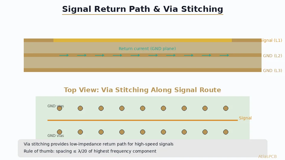
When a signal trace crosses a resonant cavity, the return path current encounters high impedance at resonance, causing:
- Impedance discontinuities — localized Z₀ variations of ±15-30%
- Radiation leakage — energy couples out through board edges
- Crosstalk amplification — cavity modes create coupling paths between unrelated traces
- Return loss degradation — S11 can spike above -10 dB at resonant frequencies
Via Stitching Design Rules
Spacing Formula
The fundamental rule: via spacing must be less than λ/20 at the highest frequency of interest.
| Frequency | λ in FR-4 (εr=4.2) | Max Via Spacing (λ/20) |
|---|---|---|
| 6 GHz | 24.4 mm | 1.22 mm |
| 10 GHz | 14.6 mm | 0.73 mm |
| 24 GHz | 6.1 mm | 0.30 mm |
| 28 GHz | 5.2 mm | 0.26 mm |
| 77 GHz | 1.9 mm | 0.095 mm |
For 77 GHz automotive radar, via spacing requirements approach the limits of mechanical drilling. Laser-drilled microvias (75-100 μm) become mandatory.
Via Geometry Selection
The via itself must present low impedance at the operating frequency:
- Drill diameter: 0.2-0.3 mm (standard) or 0.075-0.1 mm (microvia for >30 GHz)
- Pad diameter: Drill + 0.25 mm minimum annular ring
- Anti-pad: Keep anti-pad minimal (0.5 mm typical) to maximize copper plane continuity
- Aspect ratio: ≤8:1 for reliable plating; ≤1:1 for microvias
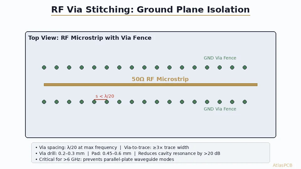
Via-to-Trace Clearance
The ground via fence must maintain adequate clearance from the signal trace to avoid impedance perturbation:
- Minimum clearance: 3× trace width
- Recommended: 4-5× trace width for sensitive 50 Ω lines
- Maximum: Keep within 2× substrate thickness to maintain shielding effectiveness
Need RF PCB Manufacturing with Tight Via Tolerances?
AtlasPCB specializes in high-frequency boards with ±0.05 mm via placement accuracy, laser-drilled microvias, and Rogers/PTFE material processing.
Get an RF PCB Quote →Via Fencing for Trace Isolation
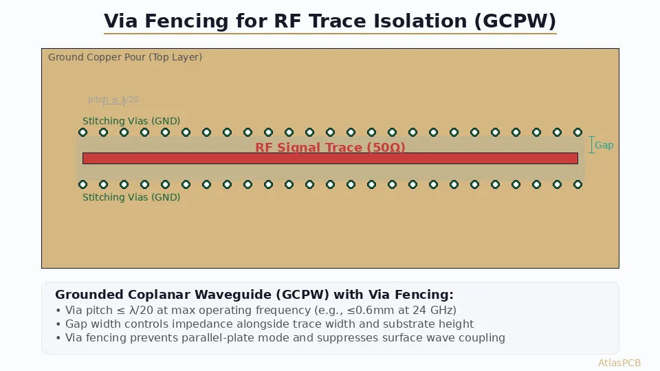
While via stitching addresses area-wide cavity suppression, via fencing creates a localized Faraday cage around individual RF traces or sensitive circuits.
Single-Row Fence Design
A single row of ground vias parallel to a signal trace provides approximately 20-30 dB of isolation below the first fence resonance frequency.
Key parameters:
- Via pitch along the fence: λ/20 maximum
- Distance from trace center: 3-5× trace width
- Via connection: Must connect all ground layers (not just adjacent)
Double-Row Fence (Enhanced Isolation)
For isolation requirements exceeding 40 dB (common in duplexer and filter sections), implement a double row:
- Offset second row by half the pitch (staggered arrangement)
- Achieves 40-60 dB isolation when properly implemented
- Required for TX/RX isolation in integrated front-end modules
Fence Termination
At the ends of via fences, EMI can leak around corners. Best practices:
- Wrap corners — Continue the via fence around 90° bends
- Extra vias at transitions — Add 2-3 additional vias where traces change direction
- Close the cage — Connect fence rows at both ends to form a complete enclosure
Implementation in Multilayer Stackups
4-Layer RF Board
For a typical 4-layer RF stackup (Signal-Ground-Ground-Signal):
- Stitch between L2 and L3 ground planes every 1-2 mm (for 10 GHz)
- Fence critical RF traces on L1 with vias connecting L2-L3-L4
- Ensure no splits in ground planes under RF routing
6+ Layer RF Board
For complex multilayer boards with multiple RF sections:
- Dedicated RF ground: Assign one plane layer exclusively for RF return current
- Cage construction: Create complete via cages around individual RF blocks
- Compartmentalization: Use via walls to divide the board into isolated RF zones (LNA, PA, mixer, LO)
Common Mistakes and How to Avoid Them
Mistake 1: Insufficient Via Density at High Frequencies
Problem: Using 2 mm via spacing for a 28 GHz design (requires 0.26 mm).
Solution: Always calculate spacing based on highest harmonic, not just fundamental. For a 28 GHz fundamental, consider up to the 3rd harmonic (84 GHz) for via stitching near non-linear components.
Mistake 2: Via Stubs Creating Resonance
Problem: Through-hole vias on inner-layer RF traces leave stubs that resonate at quarter-wavelength frequencies.
Solution: Use back-drilling to remove stubs, or use blind/buried vias. A 1 mm stub resonates at approximately 37 GHz in FR-4.
Mistake 3: Ground Plane Splits Under Via Fences
Problem: A gap in the reference plane under a via fence creates a slot antenna.
Solution: Ensure continuous ground copper under and around all via fences. Never route power traces or other signals that require plane splits in RF areas.
Mistake 4: Mixing Signal and Stitching Vias
Problem: Using the same via pattern for both signal transitions and ground stitching, creating confusion in manufacturing and increasing cost.
Solution: Clearly distinguish stitching vias in your design rules. Use a specific padstack (e.g., 0.25 mm drill, no-connect net assignment to GND) for all stitching vias.
Manufacturing Considerations
Drill Limitations
| Feature | Standard Mechanical | Laser (HDI) |
|---|---|---|
| Min drill | 0.2 mm | 0.075 mm |
| Positional accuracy | ±0.05 mm | ±0.025 mm |
| Aspect ratio | 8:1 | 1:1 |
| Cost impact | Baseline | +30-60% |
| Max frequency suitability | ~20 GHz | 77+ GHz |
Cost Optimization Strategies
- Prioritize fencing near traces — Only place dense stitching where cavity modes would impact signal paths
- Use different pitches for different zones — Dense in RF areas, relaxed in digital sections
- Combine with copper fill — Stitched copper pours are more effective than isolated via arrays
- Minimize unique drill sizes — Standardize stitching via geometry to reduce drill changes
Simulation and Verification
Pre-Layout Analysis
Before routing, perform a cavity resonance simulation:
- Define board outline and layer stackup in a 3D EM solver (HFSS, CST)
- Identify resonant modes within the operating bandwidth
- Place via stitching to shift or suppress problematic modes
- Verify with S-parameter extraction
Post-Layout Verification
After placement and routing:
- Extract the power/ground plane impedance profile (Z11 of the cavity)
- Check for impedance peaks within ±20% of operating frequency
- Verify isolation between RF compartments using coupling simulations
- Validate via fence effectiveness with near-field radiation plots
Further Reading
- Controlled Impedance PCB Design and Stackup Calculations
- PCB Hybrid Stackup: Rogers + FR-4 Integration
- Differential Impedance for PCIe Gen5 and DDR5
Ready to Manufacture Your RF PCB?
Designing high-frequency boards with aggressive via stitching requirements? AtlasPCB offers laser-drilled microvias down to 75 μm, ±0.025 mm positional accuracy, and extensive experience with Rogers, Taconic, and PTFE substrates for frequencies up to 77 GHz.
About AtlasPCB — We specialize in complex PCB manufacturing for HDI, RF, and high-reliability applications. Explore our RF and high-frequency PCB services, or get an impedance-controlled PCB manufacturing . Every order includes free engineering review. Get your quote.
Reviewed by AtlasPCB Engineering Team — IPC-certified manufacturing specialists with 15+ years of production experience in HDI, RF, and high-reliability PCB fabrication. Content based on factory floor data and real customer design reviews.
- rf pcb
- via stitching
- ground plane
- cavity resonance
- high frequency
- microwave
- signal integrity