· AtlasPCB Engineering · Engineering · 7 min read
VIPPO (Via-in-Pad Plated Over): Complete PCB Design and Manufacturing Guide
Master VIPPO technology for BGA breakout, fine-pitch components, and high-density PCB designs. Learn IPC-4761 types, manufacturing process steps, design rules, and cost optimization strategies.
What Is VIPPO Technology?
VIPPO — Via-in-Pad Plated Over — is a PCB manufacturing technique that places drilled vias directly within surface-mount component pads. The vias are filled with epoxy or conductive paste, planarized flat, then capped with an electroplated copper layer that creates a seamless, solderable surface indistinguishable from a standard pad.
This technology solves a fundamental constraint in high-density PCB design: how to route signals from fine-pitch BGAs and QFN packages without sacrificing board real estate or signal integrity. Traditional dog-bone fanout patterns consume 2-3× the area of the component footprint for routing escape. VIPPO eliminates this overhead entirely.
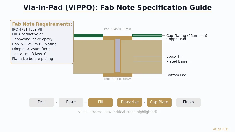
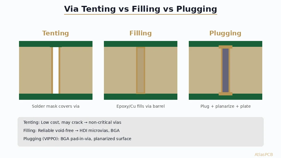
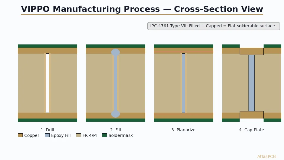
The technology is defined under IPC-4761 (Design Guide for Protection of Printed Board Via Structures), which classifies seven types of via protection. VIPPO corresponds to Type VII — filled and capped vias offering the highest reliability for demanding applications.
IPC-4761 Via Protection Types
Understanding the IPC classification helps specify the right via treatment:
| Type | Description | Application |
|---|---|---|
| Type I | Tented (dry film over via) | Low-cost consumer boards |
| Type II | Tented and covered (liquid mask) | General-purpose |
| Type III | Plugged (non-conductive fill, no cap) | Mid-reliability |
| Type IV | Plugged and covered | Automotive |
| Type V | Filled (conductive/non-conductive) | High-reliability |
| Type VI | Filled and covered (mask over fill) | BGA with mask-defined pads |
| Type VII | Filled and capped (VIPPO) | BGA direct pad, highest reliability |
For components requiring solder directly on the via, only Type VII (VIPPO) provides the flat copper surface needed for consistent solder joint formation.
VIPPO Manufacturing Process — Step by Step
The VIPPO process adds 4-6 processing steps to standard PCB fabrication:
Step 1: Drilling
Standard mechanical drilling or laser drilling creates the via hole. For VIPPO applications:
- Mechanical drill: 0.2-0.35mm diameter (aspect ratio ≤10:1)
- Laser drill (microvias): 0.075-0.15mm diameter
- Hole wall quality is critical — no nail-heading or excessive burrs
Step 2: Electroless Copper Deposition
Standard desmear and electroless copper seeds the hole walls. This provides the base conductivity for subsequent electroplating. Typical thickness: 0.5-1.0 µm.
Step 3: Pattern or Panel Plating
Electrolytic copper is plated to achieve the specified barrel thickness (typically 20-25 µm minimum per IPC-6012 Class 3). This step may occur before or after filling depending on the process flow.
Step 4: Via Filling
The critical differentiating step. Vias are filled using one of two methods:
Non-Conductive Epoxy Fill (most common):
- Screen-printed or vacuum-assisted dispensing
- Epoxy is pressed into vias from one side, with vacuum on the opposite side ensuring complete fill
- Cured at 150-170°C for 60-90 minutes
- Properties: Tg >150°C, CTE <60 ppm/°C, no outgassing during reflow
Conductive Paste Fill (for thermal vias):
- Silver or copper-filled epoxy
- Thermal conductivity: 4-15 W/mK (vs. 0.2 W/mK for standard epoxy)
- Used when via must conduct heat, not just provide routing
Step 5: Planarization
Filled vias are mechanically ground flat using ceramic or belt grinding:
- Surface flatness requirement: ≤15 µm dimple or protrusion (IPC-6012E Class 3)
- Both sides planarized simultaneously
- Critical tolerance: if dimple exceeds specification, solder paste volume varies, causing voids
Step 6: Cap Plating
A second electroplating cycle deposits 15-25 µm of copper over the filled via and surrounding pad area:
- Creates a monolithic copper surface — the filled via becomes invisible
- Adhesion between cap and filled epoxy is the most critical reliability factor
- Some fabricators use a microetch activation step before cap plating
Step 7: Surface Finish
Standard surface finish (ENIG, ENEPIG, immersion silver, etc.) is applied over the capped pads identically to standard pads.
AtlasPCB Capabilities
Need VIPPO for Your BGA Design?
We process Type VII filled-and-capped vias down to 0.2mm drill with ≤10µm planarization tolerance. Upload your Gerber files for a free DFM review.
Get a Free Quote →Design Rules for VIPPO
Pad and Via Geometry
Successful VIPPO design requires careful coordination between pad size, via diameter, and annular ring:
- Minimum pad size: Via diameter + 200 µm (100 µm annular ring per side)
- Recommended via diameter: 0.20-0.30mm for mechanical, 0.10mm for laser
- Maximum aspect ratio for reliable fill: 8:1 (deeper vias trap air during filling)
- Via-to-pad ratio: Via should be ≤60% of pad diameter
BGA Breakout with VIPPO
For fine-pitch BGAs, VIPPO enables several breakout strategies:
0.8mm pitch BGA:
- Pad diameter: 0.45mm (NSMD)
- VIPPO via: 0.25mm drill, 0.45mm pad (same as component pad)
- All signals escape on Layer 2 or deeper — no surface routing needed
0.5mm pitch BGA:
- Pad diameter: 0.30mm (NSMD)
- VIPPO via: 0.10mm laser drill (microvia)
- Microvia lands on Layer 2 capture pad: 0.30mm
- Second-level escape possible via stacked or staggered microvias
0.4mm pitch BGA:
- Requires laser-drilled microvias: 0.075-0.10mm
- Often needs stacked microvias with copper fill for reliability
- 2+N+2 or 3+N+3 HDI stackup typical
Signal Integrity Considerations
VIPPO provides inherent signal integrity advantages:
- Reduced stub length: Via barrel acts as the full-length transmission line element — no unused stub extending beyond the signal layer
- Lower parasitic capacitance: Eliminating dog-bone trace removes pad-to-ground coupling
- Shorter path length: Signal transitions vertically at the component pad rather than routing laterally to a via
- Consistent impedance: Filled via eliminates the air-dielectric discontinuity of open vias
For signals above 10 GHz, these advantages translate to measurable improvements in insertion loss and return loss.
Thermal Design with VIPPO
VIPPO vias serve dual purposes as thermal conduits:
- Array of thermal vias under exposed pad: 4-9 VIPPO vias in a grid pattern
- Fill material: Conductive paste for maximum heat transfer (4-15 W/mK)
- Connection: Vias connect exposed pad to internal or back-side copper pour
- Typical thermal improvement: 30-50% reduction in junction-to-board thermal resistance
For power components dissipating >2W, thermal VIPPO arrays are often the most practical PCB-level thermal solution without requiring copper coins or embedded heat pipes.
Common VIPPO Defects and Prevention
Dimple/Protrusion
Cause: Insufficient or excessive grinding during planarization Effect: Solder paste volume variation, head-in-pillow defects on BGA Prevention: Process control with ≤10 µm target, 100% inspection with profilometry
Epoxy Recession (Outgassing)
Cause: Via fill epoxy absorbs moisture, outgasses during reflow Effect: Solder void formation, blow-hole defects Prevention: Use low-moisture-absorption epoxy (<0.3% by weight), pre-bake boards before assembly
Cap Delamination
Cause: Poor adhesion between copper cap and filled epoxy Effect: Cap lifts during thermal cycling, creating open circuit Prevention: Microetch activation before cap plating, adequate roughness (Ra >0.3 µm)
Incomplete Fill (Void in Via)
Cause: High aspect ratio, inadequate vacuum, or epoxy viscosity issues Effect: Trapped air expands during reflow, pushing solder off pad Prevention: Vacuum-assisted filling, aspect ratio ≤8:1, optimized epoxy viscosity
VIPPO vs. Alternative Via Treatments
| Parameter | VIPPO (Type VII) | Plugged (Type III) | Tented (Type I) | Dog-Bone |
|---|---|---|---|---|
| Solderable surface | ✅ Flat copper | ❌ Not reliable | ❌ No | ✅ Separate pad |
| Assembly yield | 99.9%+ | 95-98% | <90% in-pad | 99.5% |
| Signal path length | Shortest | N/A | N/A | +1-3mm |
| Board area usage | Minimum | N/A | N/A | 2-3× pad area |
| Additional cost | +15-25% | +5-10% | +0% | +0% (but may need extra layers) |
| Thermal performance | Excellent | Poor | Poor | Good (if via nearby) |
| Suitable BGA pitch | Any | ≥1.27mm | Not for pads | ≥1.0mm |
Cost Optimization Strategies
When VIPPO Saves Money Overall
Despite the per-panel premium, VIPPO often reduces total PCB cost:
- Layer reduction: A 10-layer board with dog-bone routing may reduce to 8 layers with VIPPO, saving $5-15/board in high volume
- Board size reduction: Eliminating fanout area can shrink board dimensions 10-20%, reducing panel count
- Assembly yield improvement: Fewer solder defects means less rework cost
Specifying VIPPO Economically
- Selective VIPPO: Only fill vias in component pads — not every via on the board
- Mixed technology: VIPPO for fine-pitch BGA, standard vias elsewhere
- Design for panel efficiency: Cluster VIPPO areas to optimize filling process setup
Reliability Data
VIPPO vias per IPC-6012E Class 3 requirements:
- Thermal shock: 288°C, 6× float, no barrel cracking
- IST (Interconnect Stress Testing): >1000 cycles, <10% resistance change
- Thermal cycling: -55°C to +125°C, 1000 cycles, no cap delamination
- Humidity: 85°C/85% RH, 168 hours, no fill degradation
Major automotive and aerospace programs routinely specify VIPPO for all via-in-pad locations. IATF 16949 and AS9100 qualified fabricators maintain statistical process control on planarization depth.
Industry Applications
Automotive ADAS
Modern autonomous driving controllers use 0.5-0.65mm pitch BGAs (Mobileye EyeQ, NVIDIA Drive AGX). VIPPO enables the 16-20 layer HDI stackups these devices require while maintaining the component density needed for compact ECU form factors.
5G Infrastructure
Massive MIMO antenna arrays demand tight RF routing with minimal parasitic effects. VIPPO eliminates the stub resonances that dog-bone vias create in the 3.5-6 GHz 5G frequency bands.
Medical Implantables
Ultra-miniature hearing aids, neurostimulators, and cardiac monitors use 0.3-0.4mm pitch components on boards smaller than a postage stamp. VIPPO is the only practical interconnect method at this density.
High-Performance Computing
Server motherboards and GPU modules with HBM memory interfaces use VIPPO for the thousands of signal connections between processor and memory, where consistent impedance is critical for 8-16 Gbps signaling.
Further Reading
- BGA Fanout Routing Strategies: Dog-Bone vs Via-in-Pad
- HDI PCB Stackup Design Guide
- PCB Via Reliability Testing
- Via-in-Pad Design for BGA Components
Ready to implement VIPPO in your next design? Upload your Gerber files for a free manufacturability review. Our engineering team will verify your via-in-pad specifications meet IPC-4761 Type VII requirements and optimize for cost-effective production.
About AtlasPCB — We specialize in complex PCB manufacturing for HDI, RF, and high-reliability applications. Explore our HDI PCB manufacturing capabilities, or get an full PCB manufacturing capabilities . Every order includes free engineering review. Get your quote.
Reviewed by AtlasPCB Engineering Team — IPC-certified manufacturing specialists with 15+ years of production experience in HDI, RF, and high-reliability PCB fabrication. Content based on factory floor data and real customer design reviews.
- vippo
- via-in-pad
- pcb-manufacturing
- hdi
- bga
- ipc-4761