· AtlasPCB Engineering · Engineering · 12 min read
Embedded Component PCB Technology: Burying Passives and Actives Inside Substrates
A deep-dive into embedded component PCB technology — how resistors, capacitors, and even ICs are buried within substrate layers to slash parasitics, reclaim board space, and push high-frequency performance beyond surface-mount limits.
Embedded Component PCB Technology: Burying Passives and Actives Inside Substrates
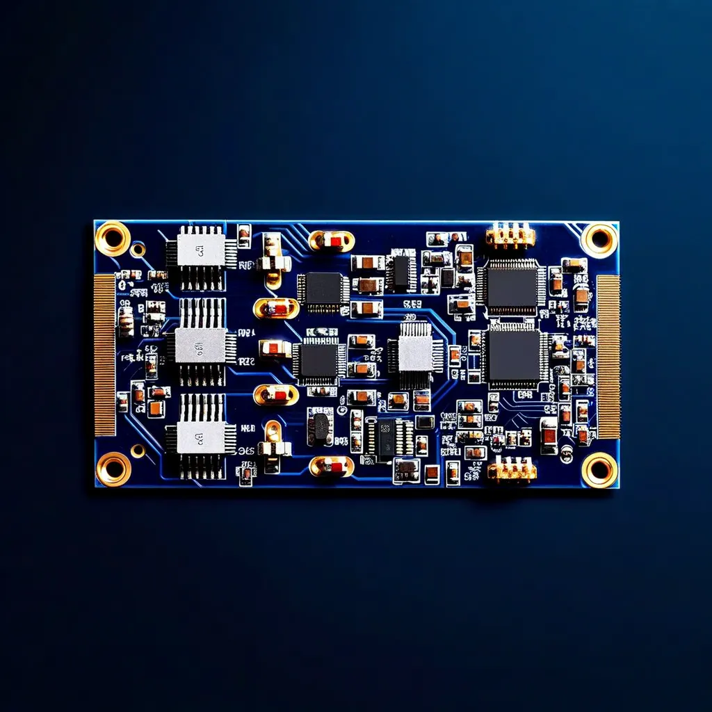
The relentless push toward smaller, faster, and more reliable electronics has forced PCB designers to rethink one of the most fundamental assumptions in board design: that components live on the surface. Embedded component technology — burying resistors, capacitors, inductors, and even bare-die ICs within the PCB substrate itself — has moved from research curiosity to production reality. Medical implants, aerospace avionics, 5G mmWave modules, and high-end smartphones now routinely use embedded passives to achieve performance levels that surface-mount technology simply cannot match.
This guide covers the materials science, manufacturing processes, design rules, and reliability considerations that every engineer needs to understand before specifying an embedded component PCB.
Why Embed Components? The Engineering Case
Surface-mount components carry inherent electrical penalties. A standard 0402 chip capacitor has 0.5–1.0 nH of mounting inductance from its solder pads and leads. At 5 GHz, that inductance creates roughly 15–30Ω of impedance — enough to severely degrade decoupling effectiveness. An embedded planar capacitor sitting directly between power and ground planes has virtually zero mounting inductance, delivering decoupling performance that no SMT capacitor can match.
The benefits extend beyond electrical performance:
- Parasitic reduction: Embedded passives eliminate solder joint inductance and pad capacitance. Signal path lengths drop by 30–50% compared to routing to surface-mount pads, directly improving [signal integrity]/blog/signal-integrity-pcb-design-guide/) in high-speed designs.
- Board real estate: In a typical smartphone RF front-end, passive components consume 60–70% of the surface area. Moving even half of these passives inside the substrate frees critical routing channels and allows smaller board outlines.
- Reliability: Eliminating solder joints removes the primary failure mechanism in vibration and thermal cycling environments. Per IPC-6012E Class 3 requirements, embedded passives avoid the solder fatigue issues that plague [BGA and QFN packages]/blog/pcb-pad-design-bga-qfn/) in harsh environments.
- Weight and thickness: Critical for wearables, implants, and aerospace applications where every gram and every 0.1mm counts.
Types of Embedded Components
Embedded Resistors
Embedded resistors are the most commercially mature embedded passive technology. Two primary material systems dominate:
Thin-Film Resistive Foils (NiCr, TaN)
Nickel-chromium (NiCr) and tantalum nitride (TaN) thin films are sputtered or electrodeposited onto copper foil before lamination. Ohmega-Ply® (NiCr) and Ticer TCR™ (TaN) are the two leading commercial products. Key specifications:
| Parameter | NiCr (Ohmega-Ply) | TaN (Ticer TCR) |
|---|---|---|
| Sheet resistance range | 25–250 Ω/sq | 25–200 Ω/sq |
| Resistor value range | 10Ω – 100kΩ | 10Ω – 50kΩ |
| TCR (temperature coefficient) | ±100 ppm/°C | ±75 ppm/°C |
| As-fabricated tolerance | ±5–10% | ±5–10% |
| Post-laser-trim tolerance | ±1% | ±1% |
| Film thickness | 50–200 Å (NiCr layer) | 100–500 Å |
The resistor geometry is defined by photolithography during inner-layer processing. Resistance is calculated as:
R = ρ_s × (L / W)
Where ρ_s is the sheet resistance (Ω/square), L is the resistor length, and W is the resistor width. A 100Ω/sq material patterned as a 10-square serpentine (L/W = 10) yields a 1kΩ resistor.
Thick-Film Polymer Resistors
Carbon-loaded polymer pastes (e.g., DuPont Interra®) are screen-printed onto inner-layer copper, then cured and laminated. Sheet resistances range from 100Ω/sq to 10kΩ/sq with ±15–20% as-fabricated tolerance. Lower precision than thin-film, but significantly lower cost. Best suited for pull-up/pull-down and termination resistors where exact values are non-critical.
Embedded Capacitors
Planar Distributed Capacitors
The simplest approach uses thin dielectric layers (12–25 µm) between adjacent power and ground planes. The [stackup design]/blog/pcb-stackup-design-guide/) incorporates a high-Dk (dielectric constant) material — typically modified epoxy with BaTiO3 ceramic filler — to maximize capacitance density.
3M™ C-Ply (Dk ≈ 16–21) and Faradflex® (Dk ≈ 7–16) are the leading commercial products. Capacitance density ranges from 0.5 nF/cm² (Dk=7, 25µm thick) to 5 nF/cm² (Dk=21, 12µm thick). This provides excellent broadband decoupling from 100 MHz to beyond 10 GHz — precisely the frequency range where discrete SMT decoupling capacitors lose effectiveness.
Discrete Embedded Capacitors
Fired ceramic capacitors (MLCC-like structures) can be embedded within cavity-routed pockets in inner layers. This approach achieves higher per-unit capacitance (up to 100 nF for a 1mm × 1mm footprint) but adds significant manufacturing complexity. It is primarily used in high-value military and medical applications.
Embedded Inductors
Spiral inductor patterns are etched on inner layers using standard photolithographic processes. Typical inductance values range from 0.5 nH to 50 nH — sufficient for RF matching networks, filters, and bias tees. Multi-layer spirals connected through [microvias]/blog/hdi-pcb-technology/) can increase inductance, though at the cost of higher parasitic capacitance and reduced self-resonant frequency.
For 5G mmWave applications operating above 24 GHz, embedded spiral inductors in low-loss substrates (Dk < 3.5, Df < 0.003) deliver Q-factors of 15–30, competitive with surface-mount chip inductors while eliminating mounting parasitics.
Embedded Active Components
The most advanced form of embedded component technology buries bare silicon die or thin-packaged ICs within the substrate. This approach, often called “chip-in-substrate” or “embedded die,” is governed by IPC-7092 Section 7 and is used in production by companies like AT&S (ECP®), TDK, and Schweizer Electronic.
The die (typically thinned to 50–100 µm) is placed face-down in a cavity or on an adhesive layer, then laminated and connected via laser-drilled microvias to the redistribution layers. This achieves:
- Shortest possible interconnects: Die-to-die signal paths of 1–3 mm vs. 10–30 mm for surface-mounted packages
- Superior thermal dissipation: The die is thermally coupled directly to copper planes and [thermal vias]/blog/pcb-thermal-via-design/)
- Extreme miniaturization: Entire systems (DC-DC converter + controller + passives) can fit within a 10mm × 10mm substrate
Manufacturing Process for Embedded Passives
The fabrication of embedded component PCBs follows a sequential build-up process that integrates seamlessly with standard [multilayer PCB manufacturing]/blog/multilayer-pcb-manufacturing-process-explained/). However, several critical additional steps are required.
Step 1: Resistive Foil Preparation
For thin-film resistors, the process begins with a laminate consisting of copper foil with a sputtered NiCr or TaN resistive layer on one side. The copper side faces outward (toward the etchant) and the resistive layer faces the dielectric core.
Step 2: Copper Patterning and Resistor Definition
Standard photolithographic processing patterns the copper layer for signal traces and resistor contact pads. A second photolithographic step then patterns the resistive layer to define resistor geometries. Critical process controls:
- Registration accuracy: ±12.5 µm (0.5 mil) between copper and resistive layer patterns to maintain resistor tolerance
- Etch uniformity: The resistive layer etching must be controlled to ±2% thickness variation across the panel to maintain sheet resistance uniformity
- Minimum resistor width: 100 µm (4 mil) for production; 50 µm (2 mil) for advanced processes
Step 3: Capacitor Dielectric Lamination
For planar embedded capacitors, a thin high-Dk dielectric sheet (12–25 µm C-Ply or Faradflex) is laminated between designated power/ground plane pairs during the standard lamination cycle. No additional processing steps are needed — the capacitor structure is inherently formed by the plane pair geometry.
Step 4: Sequential Lamination and Via Formation
The embedded component layers are incorporated into the full [stackup]/blog/pcb-stackup-design-guide/) through sequential lamination. Laser-drilled microvias connect embedded components to adjacent signal and power layers. Via landing pads on embedded resistors must be ≥200 µm (8 mil) diameter to ensure reliable connection to the thin resistive film.
Step 5: Laser Trimming (Optional)
Post-fabrication laser trimming can improve embedded resistor tolerance from ±10% to ±1%. A probe contacts the resistor terminals while a YAG or CO2 laser ablates the resistive film in a controlled serpentine or L-cut pattern, progressively increasing resistance until the target value is reached. Trimming adds cost ($0.02–0.05 per resistor) but is essential for precision analog circuits.
Step 6: Standard Outer-Layer Processing
The remainder of the fabrication follows standard multilayer processing: outer-layer imaging, plating, [surface finish]/blog/pcb-surface-finish-comparison-2026/) application (ENIG recommended for embedded component boards due to its planarity), solder mask, and routing.
Design Rules and Guidelines per IPC-7092
IPC-7092 (“Design and Assembly Process Implementation for Embedded Components”) provides comprehensive guidance. Key design rules include:
Resistor Layout Rules
- Minimum resistor width: 100 µm (0.1 mm / 4 mil)
- Minimum resistor length: 100 µm (0.1 mm / 4 mil)
- Contact pad overlap: ≥50 µm beyond resistor body on each end
- Keep-out from via pads: ≥200 µm from resistor body edge to nearest via pad
- Keep-out from board edge: ≥500 µm from resistor body to rout/score line
- Maximum L/W ratio: 20:1 (higher ratios cause unacceptable tolerance spread)
- Serpentine spacing: ≥100 µm between parallel resistor segments
Capacitor Layout Rules
- Minimum plane overlap: Capacitor plane pair must extend ≥500 µm beyond the required capacitance area to account for registration
- Anti-pad clearance: Signal vias passing through capacitor plane pairs require standard anti-pad clearances per [impedance control]/blog/pcb-impedance-control/) requirements
- No copper splits: Capacitor planes should be solid copper (no splits, slots, or thermal relief patterns) within the capacitance zone
Embedded Die Rules (per IPC-7092 Section 7)
- Cavity depth tolerance: ±15 µm
- Die placement accuracy: ±25 µm
- Die-to-cavity wall clearance: ≥50 µm on all sides
- Microvia landing pad on die pads: ≥100 µm diameter
- Maximum die thickness: 100 µm (preferred 50 µm for reliable lamination fill)
Reliability and Qualification
Embedded components must meet stringent reliability requirements, particularly for IPC-6012E Class 3 (high-reliability) applications.
Thermal Cycling Performance
Embedded thin-film resistors demonstrate exceptional thermal stability. Per IPC-2316 qualification testing:
- Temperature cycling (-55°C to +125°C, 1000 cycles): Resistance change < ±0.5% for NiCr, < ±1.0% for TaN
- Thermal shock (-65°C to +150°C, 100 cycles): Resistance change < ±1.0%
- Moisture resistance (85°C/85% RH, 1000 hours): Resistance change < ±1.5%
- Biased humidity (85°C/85% RH, 100V DC, 1000 hours): Resistance change < ±2.0%
These numbers compare very favorably to the ±0.25–0.5% drift typical of discrete SMT chip resistors under the same conditions. The absence of solder joints eliminates the primary fatigue failure mechanism.
Long-Term Stability
Accelerated aging studies show embedded NiCr resistors drift less than ±0.1% per year at 70°C continuous operating temperature. This stability makes embedded resistors suitable for precision instrumentation, medical devices, and [high-reliability applications]/blog/pcb-via-reliability-testing/) requiring 20+ year service life.
Known Failure Modes
- Resistive film delamination: Caused by inadequate surface preparation before lamination or excessive moisture absorption. Controlled by proper prebake (4h at 105°C) and vacuum lamination.
- Laser trim cracking: Overtrimming or improper trim geometry can create stress concentration points that propagate under thermal cycling. L-cuts are preferred over plunge cuts for improved reliability.
- Embedded die cracking: Thin die (< 50 µm) are susceptible to cracking from CTE mismatch during lamination. Proper cavity fill material selection (low-CTE adhesive) and controlled pressure profiles mitigate this risk.
High-Frequency Advantages
For RF and mmWave applications, embedded components offer compelling advantages:
Parasitic Elimination
A surface-mount 0402 resistor has approximately 0.3 nH of inductance and 0.05 pF of pad capacitance. At 28 GHz (5G NR FR2), this creates significant impedance perturbation. An embedded thin-film resistor of equivalent value has < 0.05 nH inductance and negligible pad capacitance, maintaining its designed impedance to beyond 40 GHz.
Distributed Filter Design
Embedded components enable filter topologies impossible with discrete parts. A bandpass filter combining embedded spiral inductors and planar capacitors on a low-loss substrate ([Rogers or Taconic materials]/blog/pcb-materials-guide/)) can achieve insertion loss < 0.5 dB with Q-factors exceeding 50 at 5 GHz — performance approaching LTCC (Low-Temperature Co-fired Ceramic) at a fraction of the cost.
Power Distribution Network (PDN) Optimization
Planar embedded capacitance layers provide inherent broadband decoupling across the entire board area. Combined with proper [copper weight selection]/blog/pcb-copper-weight-thickness/) for low-impedance power planes, embedded capacitance can reduce the number of discrete decoupling capacitors by 30–50%, simplifying assembly and improving reliability.
Design for Test (DFT) Considerations
Testing embedded components presents unique challenges since the components are, by definition, inaccessible after lamination.
In-Process Testing
Embedded resistors should be electrically tested at the inner-layer stage, before lamination. Flying probe or fixture-based testing measures resistance values and identifies opens/shorts. This is the last opportunity to identify resistor defects before they become buried.
Post-Lamination Testing
After lamination, embedded resistors are accessed through their connected circuit nets. Standard ICT (In-Circuit Test) cannot probe individual embedded resistors unless dedicated test pads are designed into the net. Best practice: include at least one accessible test point per embedded resistor net.
Design Recommendations for Testability
- Add test pads (minimum 0.5 mm diameter) connected to each end of every embedded resistor
- Place test pads on accessible outer layers
- Include at least 2mm spacing between test pads for flying probe access
- Document embedded component locations in the fabrication notes with layer references
- Specify embedded resistor nominal values and tolerances in the BOM for comparison against measured values
Cost Considerations
Embedded component PCBs carry a cost premium over standard multilayer boards, but the system-level economics often favor embedding:
| Cost Factor | Impact |
|---|---|
| Resistive foil material | +15–25% over standard copper foil |
| Additional photolithographic steps | +$100–300 per panel |
| Laser trimming (if required) | +$0.02–0.05 per resistor |
| Reduced SMT assembly (fewer placements) | -10–30% assembly cost |
| Smaller board outline (less material) | -5–15% board cost |
| Improved yield (fewer solder defects) | -3–8% rework/scrap cost |
For designs with > 200 passive components per board, the assembly cost savings alone can offset the substrate cost premium. The breakeven point depends on component density, board volume, and the specific tolerance requirements.
When to Use (and When Not to Use) Embedded Components
Best applications for embedded passives:
- 5G mmWave front-end modules (parasitic-critical)
- Medical implants (size and reliability critical)
- Aerospace avionics (vibration reliability, IPC Class 3)
- High-density SiP (System-in-Package) substrates
- Power integrity improvement for high-speed digital (PDN decoupling)
Not recommended for:
- Designs requiring ±0.1% resistor tolerance (use SMT precision parts)
- Low-volume prototypes (NRE cost is high)
- Simple designs with adequate surface space
- Designs where frequent BOM changes are expected (embedded components are fixed at fabrication)
Conclusion
Embedded component PCB technology represents a fundamental shift in how we think about the relationship between components and substrate. By burying passives — and increasingly, actives — within the PCB itself, engineers can achieve electrical performance, miniaturization, and reliability levels that surface-mount technology cannot match. The technology is mature, the standards (IPC-7092, IPC-2316) are well-established, and the manufacturing ecosystem supports production volumes from prototype through high-volume.
For designs where parasitics, board space, or solder joint reliability are limiting factors, embedded components deserve serious evaluation as part of your [HDI PCB technology]/blog/hdi-pcb-technology/) strategy.
Ready to start your project? Upload your Gerbers for a free engineering review, or talk to an engineer about your design requirements.
Further Reading
- [HDI PCB Design Guide: Stackup Rules, Via Structures & DFM Checklist]/blog/hdi-pcb-design-guide/)
- [PCB Sequential Lamination: Process, Design Rules, and When You Need It]/blog/pcb-sequential-lamination/)
- [High-Speed PCB Design: Signal Integrity Essentials for Modern Electronics]/blog/high-speed-pcb-design/)
- [Multilayer PCB Stackup Design Guide: 8 to 30+ Layers Step by Step]/blog/multilayer-pcb-stackup-design-guide/)
- [PCB Manufacturer with Engineering Review: Why Human DFM Audit Matters]/blog/pcb-manufacturer-engineering-review/)
About AtlasPCB — We specialize in complex PCB manufacturing for HDI, RF, and high-reliability applications. Explore our full PCB manufacturing capabilities, or get an instant online quote . Every order includes free engineering review. Get your quote.
Reviewed by AtlasPCB Engineering Team — IPC-certified manufacturing specialists with 15+ years of production experience in HDI, RF, and high-reliability PCB fabrication. Content based on factory floor data and real customer design reviews.
- embedded-components
- advanced-packaging
- pcb-technology
- miniaturization