· AtlasPCB Engineering · Engineering · 14 min read
PCB Thermal Via Design: Engineering Guide to Heat Dissipation Through Via Arrays
Complete engineering guide to thermal via design for power components. Covers via diameter and pitch calculations, IPC-2152 thermal guidelines, thermal resistance formulas, filled vs unfilled vias, and ANSYS simulation best practices.

PCB Thermal Via Design: Engineering Guide to Heat Dissipation Through Via Arrays
Thermal management is one of the most critical — and most frequently under-designed — aspects of modern PCB engineering. As power densities increase with smaller packages like QFN, DFN, and high-current MOSFETs, the exposed thermal pad on the component underside becomes the primary heat path. The only way to effectively extract that heat through the PCB substrate is with properly designed thermal via arrays.
This guide provides a complete engineering reference for thermal via design, covering geometry optimization, thermal resistance calculations, IPC standard compliance, fill material selection, and simulation methodology. Whether you’re designing LED drivers dissipating 3W or power converters handling 50W+, the principles here apply directly to your layout.
Why Thermal Vias Matter: The Physics of PCB Heat Transfer
FR-4 is a terrible thermal conductor. With a through-plane thermal conductivity of just 0.3–0.4 W/m·K (compared to copper’s 390 W/m·K), a standard 1.6mm FR-4 substrate acts as an effective thermal insulator. For a component dissipating even modest power — say 2W over a 5×5mm thermal pad — the temperature rise through the FR-4 alone would be:
ΔT = P × L / (k × A) ΔT = 2 × 0.0016 / (0.35 × 25×10⁻⁶) = 365°C
That’s clearly unacceptable. Thermal vias solve this by creating copper pathways through the board, dramatically reducing the thermal resistance from the component pad to internal copper planes and the bottom side of the PCB.
The Three Heat Transfer Mechanisms in PCBs
Conduction through copper — Primary mechanism. Thermal vias, copper planes, and copper pours conduct heat laterally and vertically. Copper’s thermal conductivity (390 W/m·K) is roughly 1000× that of FR-4.
Convection from surfaces — Secondary mechanism. Heat reaching the bottom copper layer or internal planes eventually dissipates via natural or forced convection. Typical convection coefficients: 5–25 W/m²·K (natural) or 25–100 W/m²·K (forced air).
Radiation — Minimal contribution at PCB operating temperatures (< 125°C). Typically < 5% of total heat dissipation in enclosed systems.
The thermal via array’s job is to maximize mechanism #1 — getting heat from the top-side component pad to copper planes and the bottom surface where mechanisms #2 and #3 can do their work.
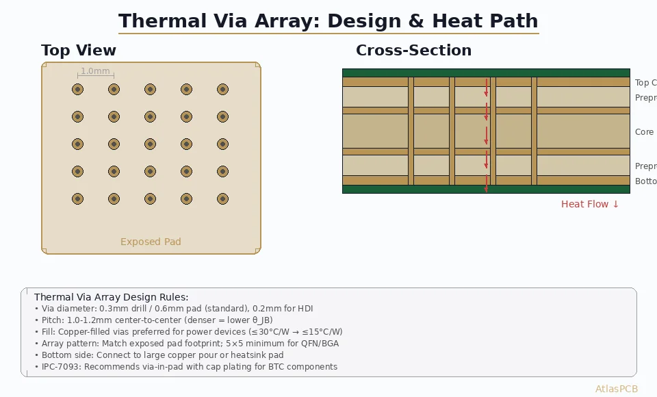
Thermal Via Geometry: Diameter, Pitch, and Array Design
Via Diameter Selection
The thermal conductance of a single plated via is proportional to the cross-sectional area of the copper annulus. For a standard via with drill diameter d and plating thickness t:
A_copper = π × t × (d - t)
For typical parameters:
- 0.2mm drill, 25μm plating: A = π × 0.025 × (0.2 - 0.025) = 13.7 × 10⁻⁹ m²
- 0.3mm drill, 25μm plating: A = π × 0.025 × (0.3 - 0.025) = 21.6 × 10⁻⁹ m²
- 0.4mm drill, 25μm plating: A = π × 0.025 × (0.4 - 0.025) = 29.5 × 10⁻⁹ m²
The 0.3mm drill offers the best compromise between thermal performance and manufacturability. Smaller vias (0.2mm) increase drilling cost and reduce copper area; larger vias (0.4mm+) risk excessive solder wicking and reduce the number of vias that fit in a given pad area.
Recommendation: Use 0.3mm (12 mil) finished drill diameter for thermal vias as a standard starting point. For [HDI designs]/blog/hdi-pcb-technology/) requiring microvias, 0.15mm laser-drilled vias can be used but require copper filling for thermal effectiveness.
Via Pitch Optimization
Via pitch determines the array density. The constraints are:
- Minimum pitch (manufacturing): Typically 0.8mm for 0.3mm drill (IPC-2221B minimum annular ring of 0.125mm + drill tolerance)
- Optimal pitch (thermal): 1.0–1.2mm center-to-center provides a good balance
- Maximum pitch: Beyond 1.5mm, the FR-4 between vias dominates thermally and performance degrades
For a 5×5mm QFN thermal pad with 1.0mm pitch, you can fit a 5×5 = 25 via array. At 1.2mm pitch, you get 4×4 = 16 vias. The thermal resistance difference between these two arrays is significant:
| Array | Via Count | R_thermal (1.6mm board) | R_thermal (1.0mm board) |
|---|---|---|---|
| 5×5 @ 1.0mm | 25 | 6.7°C/W | 4.2°C/W |
| 4×4 @ 1.2mm | 16 | 10.4°C/W | 6.5°C/W |
| 3×3 @ 1.5mm | 9 | 18.5°C/W | 11.6°C/W |
Array Pattern Design Rules
- Fill the thermal pad area — Place vias across the entire exposed pad footprint, not just the center
- Maintain uniform spacing — Non-uniform arrays create thermal hotspots
- Offset from pad edges — Keep vias at least 0.3mm from the pad edge to maintain solder mask dam integrity
- Align with internal plane connections — Ensure vias connect to continuous copper pours on inner layers, not isolated thermal reliefs. Refer to the [PCB stackup design guide]/blog/pcb-stackup-design-guide/) for optimal plane placement
Thermal Resistance Calculations: From Single Via to Complete Thermal Path
Single Via Thermal Resistance
For a plated-through via with no fill:
R_via = L / (k_Cu × A_annulus)
Where:
- L = board thickness (m)
- k_Cu = 390 W/m·K
- A_annulus = π × t × (d - t)
Example: 0.3mm drill, 25μm plating, 1.6mm board:
- A = π × 0.025 × 10⁻³ × (0.3 - 0.025) × 10⁻³ = 21.6 × 10⁻⁹ m²
- R_via = 0.0016 / (390 × 21.6 × 10⁻⁹) = 190°C/W
Copper-Filled Via Thermal Resistance
For a copper-filled via (IPC-4761 Type VII):
R_filled = L / (k_Cu × A_total)
Where A_total = π × (d/2)²
Example: 0.3mm copper-filled via, 1.6mm board:
- A = π × (0.15 × 10⁻³)² = 70.7 × 10⁻⁹ m²
- R_filled = 0.0016 / (390 × 70.7 × 10⁻⁹) = 58°C/W
Copper filling reduces single-via thermal resistance by approximately 3.3× compared to hollow plated vias.
Via Array Parallel Resistance
For N identical vias in parallel:
R_array = R_via / N
A 4×4 array of copper-filled 0.3mm vias: R_array = 58 / 16 = 3.6°C/W
Complete Thermal Path
The total junction-to-ambient thermal resistance includes:
R_θJA = R_θJC + R_contact + R_via_array + R_spreading + R_convection
Where:
- R_θJC = junction-to-case (from component datasheet, typically 1–10°C/W)
- R_contact = solder joint resistance (typically 0.5–2°C/W)
- R_via_array = as calculated above
- R_spreading = lateral spreading in copper planes (1–5°C/W depending on area)
- R_convection = surface-to-air (highly dependent on airflow and heatsink)

IPC Standards for Thermal Via Design
IPC-2152: Standard for Determining Current-Carrying Capacity
IPC-2152 supersedes the older IPC-2221 current tables and provides a more accurate thermal model for PCB conductors. Key thermal guidelines relevant to via design:
- Ambient temperature derating: Maximum allowable temperature rise must account for the worst-case ambient. For automotive applications (IPC-6012DA), ambient can reach 125°C, leaving only 25°C rise to hit the 150°C FR-4 Tg limit.
- Thermal coupling between conductors: Adjacent vias share heat paths through the FR-4 between them. IPC-2152 charts show that closely-spaced vias (< 1mm pitch) have diminishing returns due to thermal interaction.
- Board thickness impact: Thinner boards have lower via thermal resistance (linear relationship), making 1.0mm boards significantly better than 1.6mm for thermal via applications.
IPC-4761: Design Guide for Protection of Printed Board Via Structures
IPC-4761 defines seven types of via protection, of which three are relevant to thermal via applications:
| Type | Description | Thermal Conductivity | Use Case |
|---|---|---|---|
| Type V | Filled with non-conductive material, not capped | 0.2–0.8 W/m·K | Low-cost, minimal thermal benefit |
| Type VI | Filled with conductive material, not capped | 1–10 W/m·K (silver epoxy) | Good thermal performance, moderate cost |
| Type VII | Filled with copper, planarized and capped | 390 W/m·K | Best thermal performance, highest cost |
For power applications dissipating > 2W, Type VII (copper-filled) is strongly recommended. The difference in thermal performance between conductive epoxy (Type VI) and solid copper (Type VII) is 40–400×, which translates directly to junction temperature reduction.
IPC-6012: Qualification and Performance Specification
IPC-6012 Class 3 (high reliability) imposes additional requirements on thermal vias:
- Minimum copper plating thickness: 25μm in the via barrel (IPC-6012 §3.6.2.4)
- Barrel crack resistance: Must withstand 6× thermal cycling (-65°C to +125°C) without failure per IST testing
- Via fill void limit: For filled vias, maximum void percentage is 25% of the via cross-section for Class 3
These requirements are critical for automotive, aerospace, and medical applications where thermal vias must maintain long-term reliability. Understanding [via reliability testing]/blog/pcb-via-reliability-testing/) methodology is essential for mission-critical designs.
Filled vs. Unfilled Thermal Vias: Design Tradeoffs
Unfilled (Open) Thermal Vias
Advantages:
- Lowest manufacturing cost
- No additional process steps
- Suitable for wave-soldered through-hole assemblies
Disadvantages:
- Solder wicking during reflow (solder flows down through the via, starving the pad joint)
- Air column in via barrel has extremely poor thermal conductivity (0.025 W/m·K)
- Can cause voiding under BGA and QFN thermal pads
- Solder balls may form on the bottom side during reflow
Mitigation for unfilled vias: Use solder mask tenting on the bottom side (via-in-pad with bottom-side tenting). However, this creates a trapped air pocket and may not survive thermal cycling without delamination.
Epoxy-Filled Thermal Vias (IPC-4761 Type V/VI)
Non-conductive epoxy fill (Type V) provides mechanical stability and prevents solder wicking, but offers negligible thermal improvement over air. Thermal conductivity of standard epoxy fill: 0.2–0.8 W/m·K.
Conductive epoxy fill (Type VI) uses silver or copper particle-loaded epoxy with thermal conductivity of 1–10 W/m·K. This provides moderate thermal improvement at reasonable cost:
- Silver-loaded epoxy: 3–10 W/m·K
- Copper-loaded epoxy: 1–5 W/m·K
- Carbon-loaded epoxy: 1–3 W/m·K
Copper-Filled Thermal Vias (IPC-4761 Type VII)
Copper electroplating fills the entire via barrel, achieving thermal conductivity of 390 W/m·K — the same as bulk copper. The via is then planarized (ground flat) and optionally capped with additional copper plating.
Process steps:
- Standard drilling and desmear
- Electroless copper seed layer
- Electrolytic copper fill plating (specialized pulse-reverse plating chemistry)
- Planarization (mechanical grinding or chemical-mechanical polishing)
- Optional: cap plating with additional 15–25μm copper
- Standard outer layer processing continues
Cost impact: Copper-filled vias add approximately 15–25% to the base PCB fabrication cost, depending on via count and board thickness. For boards already requiring [HDI stackup processing]/blog/hdi-pcb-stackup-design-advanced/), the incremental cost is lower since similar fill processes are already in the flow.
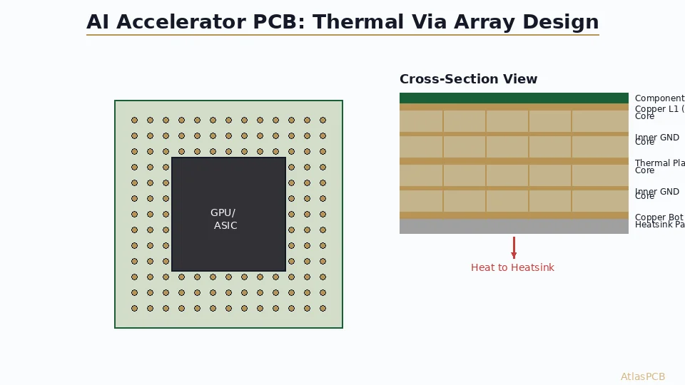
Design Guidelines for Specific Components
QFN / DFN Packages
QFN packages rely almost entirely on the exposed thermal pad for heat dissipation. Typical design rules:
- Via array: Fill the entire thermal pad area with 0.3mm vias on 1.0mm pitch
- Via fill: Copper fill (Type VII) or conductive epoxy (Type VI) mandatory
- Solder paste: Use 50-75% paste coverage on the thermal pad to prevent voiding
- Bottom-side copper: Mirror the thermal pad area with a copper pour on the bottom layer, connected to the via array
- Inner planes: Connect vias to at least one internal ground plane for lateral heat spreading
Example: Texas Instruments LM5146 (QFN-40, 6×6mm thermal pad, 3.5W typical dissipation):
- Thermal pad area: 36mm²
- Via array: 6×6 = 36 vias at 0.9mm pitch (copper-filled)
- Calculated R_via_array: 36 vias × 58°C/W each = 1.6°C/W
- Junction temperature at 25°C ambient: T_J = 25 + 3.5 × (3.2 + 0.5 + 1.6 + 2.0 + 15) = 103°C (within 125°C limit)
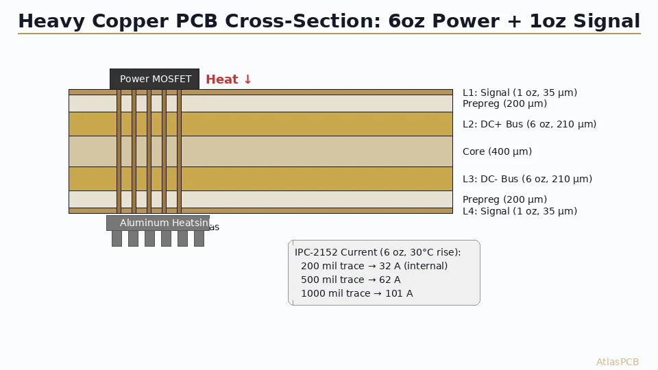
Power MOSFETs (D2PAK, DPAK, PowerPAK)
Power MOSFETs in surface-mount packages often dissipate 10–50W. The thermal design is more aggressive:
- Via array: Maximum density under the drain pad
- Copper weight: Use 2oz (70μm) or heavier copper on outer layers
- Bottom heatsink: Direct connection to external heatsink via thermal interface material
- Thermal relief: Do NOT use thermal relief patterns on internal plane connections — use full-flood connections for minimum thermal resistance
High-Power LED Drivers
LED driver modules present unique challenges because the [thermal management approach]/blog/pcb-thermal-management/) must handle both the driver IC power dissipation and the thermal path to LED arrays:
- Metal-core PCB (MCPCB) alternative: For LED applications > 10W, consider aluminum or copper-core substrates instead of FR-4 with thermal vias
- Hybrid approach: FR-4 main board with thermal vias under driver IC, connected to aluminum heatsink bracket
- Via array under inductor: Don’t forget the power inductor — it can dissipate 0.5–2W in switching converters
Thermal Simulation Best Practices
ANSYS Icepak / Mechanical Thermal
For accurate thermal via modeling in ANSYS:
- Don’t model individual vias at board level — Use equivalent thermal conductivity for the via array region instead. The effective through-plane conductivity of a via array can be calculated as:
k_eff = k_Cu × A_via_total / A_pad + k_FR4 × (1 - A_via_total / A_pad)
For a 0.3mm copper-filled via array at 1.0mm pitch:
- Via area ratio: π(0.15)² / (1.0)² = 7.07%
- k_eff = 390 × 0.0707 + 0.35 × 0.9293 = 27.9 W/m·K (vs 0.35 for plain FR-4)
Model internal planes explicitly — The lateral spreading in copper planes dominates the far-field thermal behavior. A continuous 1oz copper plane provides approximately 40× the lateral conductivity of FR-4.
Include convection boundaries — Apply appropriate heat transfer coefficients:
- Natural convection (still air): 5–10 W/m²·K
- Low-velocity forced air (1 m/s): 25 W/m²·K
- High-velocity forced air (3 m/s): 50–75 W/m²·K
Validate with thermal test coupons — Fabricate test boards with thermocouples embedded near the thermal via array. Compare measured vs simulated temperatures within ±10%.
Simplified Hand Calculations
For quick estimates without simulation, use the thermal resistance network:
- Calculate R_via_array as described above
- Estimate R_spreading using the Kennedy formula: R_spread = 1 / (π × k × d_source) × (1 - r_source/r_spread)
- Look up R_θJC from the component datasheet
- Calculate R_convection = 1 / (h × A_surface)
- Sum the series resistances and multiply by power dissipation
This method is typically accurate to ±20%, sufficient for initial design and [Gerber file preparation]/blog/pcb-gerber-files-guide/) before committing to detailed simulation.
Common Thermal Via Design Mistakes
Mistake 1: Thermal Relief on Internal Connections
Using thermal relief (spoke) connections between thermal vias and internal planes defeats the purpose. Each spoke connection adds approximately 5–15°C/W of resistance. Always use full-flood (direct) connections for thermal vias on internal planes.
Exception: If the via also carries signal or the plane is used for power distribution, thermal relief may be needed to prevent solder drainage during assembly. In this case, use 4-spoke relief with 0.3mm spoke width (wider than default).
Mistake 2: Insufficient Via Count
A single 0.3mm via under a QFN pad provides ~190°C/W (unfilled) or ~58°C/W (copper-filled). For a component dissipating 3W, that’s 570°C or 174°C temperature rise — clearly inadequate. You need arrays of 9–25+ vias.
Mistake 3: Ignoring Solder Wicking
Open (unfilled) vias under SMT pads will wick solder during reflow, creating:
- Starved solder joints on the component pad
- Solder balls on the bottom side
- Reduced thermal contact area
Always specify via fill for thermal vias under SMT pads. If cost is a concern, at minimum use non-conductive epoxy fill with top-side cap plating.
Mistake 4: Forgetting the Bottom-Side Copper
Thermal vias are only half the solution. The bottom side needs adequate copper area to dissipate heat into the ambient. Design rules:
- Bottom copper pour area: ≥ 4× the component thermal pad area
- Connect to ground plane for maximum spreading area
- Consider [surface finish selection]/blog/pcb-surface-finish-comparison-2026/) — bare copper oxidizes and reduces emissivity
Mistake 5: Not Considering Board Thickness
Board thickness directly affects thermal via resistance (linear relationship). If thermal management is critical:
- Use 1.0mm board thickness instead of 1.6mm (37.5% reduction in via thermal resistance)
- Use 0.8mm for extreme cases (requires mechanical stiffening considerations)
- Thinner boards also improve the effectiveness of the overall [multilayer manufacturing process]/blog/multilayer-pcb-manufacturing-process-explained/)
Advanced Techniques: Coin Insertion and Embedded Heatsinks
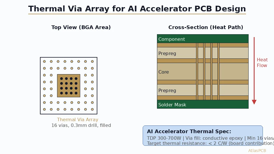
For applications where even optimized thermal via arrays are insufficient (typically > 20W in a localized area), consider:
Copper Coin (Slug) Technology
A solid copper coin (typically 1–3mm thick, matching the component footprint) is press-fit into a routed pocket in the PCB. This replaces the FR-4 under the component entirely:
- Thermal resistance: < 1°C/W for a 10×10mm coin
- Additional cost: $3–10 per board (depending on coin size and quantity)
- Requires precise pocket routing and press-fit insertion during lamination
- Must maintain coplanarity within ±50μm
Heavy Copper Inner Layers
Using 3oz (105μm) or 4oz (140μm) copper on inner layers adjacent to the thermal via array improves lateral spreading significantly. The thermal spreading resistance drops proportionally with copper thickness.
Summary: Thermal Via Design Decision Matrix
| Power Level | Recommended Approach | Via Spec | Fill Type |
|---|---|---|---|
| < 1W | Standard via array | 0.3mm, 1.2mm pitch | Epoxy fill (Type V) |
| 1–5W | Dense via array | 0.3mm, 1.0mm pitch | Conductive epoxy (Type VI) |
| 5–15W | Maximum density + thick copper | 0.3mm, 0.9mm pitch, 2oz Cu | Copper fill (Type VII) |
| 15–30W | Copper fill + bottom heatsink | 0.3mm, 0.9mm pitch, 2oz Cu | Copper fill (Type VII) |
| > 30W | Copper coin or MCPCB | N/A | N/A |
Proper thermal via design is essential for reliable [power electronics PCBs]/blog/pcb-pad-design-bga-qfn/). By applying the calculations, IPC standards, and design rules in this guide, you can ensure your thermal via arrays deliver the heat dissipation performance your design requires — and avoid the costly thermal failures that plague under-designed boards.
Ready to start your project? Upload your Gerbers for a free engineering review, or talk to an engineer about your design requirements.
Further Reading
- [HDI PCB Design Guide: Stackup Rules, Via Structures & DFM Checklist]/blog/hdi-pcb-design-guide/)
- [How to Design an HDI Stackup: Step-by-Step for First-Time Designers]/blog/how-to-design-hdi-stackup/)
- [Via-in-Pad Design: Filled, Capped, and Plated Over — Complete Guide]/blog/via-in-pad-design/)
- [Multilayer PCB Stackup Design Guide: 8 to 30+ Layers Step by Step]/blog/multilayer-pcb-stackup-design-guide/)
- [PCB Manufacturer with Engineering Review: Why Human DFM Audit Matters]/blog/pcb-manufacturer-engineering-review/)
About AtlasPCB — We specialize in complex PCB manufacturing for HDI, RF, and high-reliability applications. Explore our aluminum and metal-core PCB services . Every order includes free engineering review. Get your quote.
Reviewed by AtlasPCB Engineering Team — IPC-certified manufacturing specialists with 15+ years of production experience in HDI, RF, and high-reliability PCB fabrication. Content based on factory floor data and real customer design reviews.
- thermal-management
- via-design
- pcb-design
- power-electronics