· AtlasPCB Engineering · Engineering · 8 min read
PCB Inner Layer Oxide Treatment: Black Oxide vs Brown Oxide Adhesion for Multilayer Reliability
Compare black oxide (CuO) and brown oxide (Cu₂O) treatments for PCB inner layer adhesion. Learn peel strength data, pink ring prevention, reduced oxide alternatives, and IPC-TM-650 testing methods.

The Hidden Layer That Holds Your PCB Together
Every multilayer PCB relies on a chemical bond between copper and resin that is invisible in the finished product but absolutely critical to reliability. When inner layer copper panels are laminated with prepreg (partially cured resin sheets) under heat and pressure, the resin must flow into and mechanically interlock with the copper surface. A smooth, untreated copper surface bonds poorly — peel strength may be only 2–3 lb/in, well below the minimum for reliable operation.
Inner layer oxide treatment transforms the smooth copper surface into a micro-rough, chemically reactive surface that the resin can grip. The quality of this treatment determines whether the multilayer PCB will survive [thermal cycling]/blog/hdi-via-reliability-thermal-cycling/), lead-free reflow soldering, and years of operation without delamination.
Black Oxide (CuO): The Traditional Approach
Chemistry and Process
Black oxide treatment converts the surface of the copper into cupric oxide (CuO) through a controlled alkaline oxidation process:
Process sequence:
- Clean — Remove organics, fingerprints, and oxidation with alkaline cleaner
- Micro-etch — Light etch (sodium persulfate or sulfuric acid/peroxide) to create initial roughness and expose fresh copper
- Oxidize — Immerse in hot alkaline oxidizing solution (sodium hydroxide + sodium chlorite + trisodium phosphate) at 70–85°C for 2–5 minutes
- Rinse and dry — Thorough water rinse followed by forced-air drying
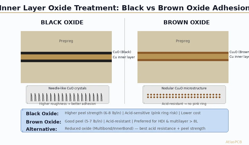
The CuO layer forms as needle-like crystal structures approximately 1–3 µm tall, creating a high surface area that the prepreg resin can flow around and mechanically interlock with during lamination. The resulting copper-to-resin bond relies primarily on this mechanical interlocking rather than chemical adhesion.
Performance Characteristics
| Property | Black Oxide (CuO) | Measurement Method |
|---|---|---|
| Crystal structure | Needle-like, 1–3 µm height | SEM imaging |
| Color | Deep black/dark brown | Visual |
| Peel strength (as laminated) | 6–8 lb/in | IPC-TM-650, 2.4.8 |
| Peel strength (after thermal stress) | 5–7 lb/in | After 6× solder float |
| Acid resistance | Poor | Dissolves in pH < 3 |
| Pink ring risk | High | IPC-A-600 inspection |
| Process temperature | 70–85°C | — |
| Treatment time | 2–5 min | — |
The Pink Ring Problem
The Achilles heel of black oxide is its vulnerability to acid. CuO dissolves readily in the acidic solutions used during subsequent PCB processing steps:
- Desmear/etchback (permanganate or plasma)
- Electroless copper deposition (highly acidic catalyst and electroless bath)
- Acid cleaning between plating steps
When acid contacts the CuO layer at the drill hole wall, it dissolves the oxide along the copper-resin interface by capillary action, creating the characteristic pink ring — a halo of exposed bare copper visible around the drilled hole when viewed from the inner layer.
Pink ring is more than cosmetic:
- It indicates a weakened copper-resin bond at the hole wall
- It can propagate into delamination under thermal stress
- It is a rejectable defect per IPC-A-600 Class 3
Brown Oxide (Cu₂O): The Acid-Resistant Alternative
Chemistry and Process
Brown oxide converts the copper surface to cuprous oxide (Cu₂O) instead of cupric oxide. The key difference is in the oxidizing chemistry — brown oxide processes use a milder, controlled reaction that produces a denser, nodular oxide structure:
Process sequence:
- Clean — Similar to black oxide
- Micro-etch — Creates initial roughness
- Oxidize — Modified alkaline solution at lower temperature (50–65°C), producing Cu₂O instead of CuO
- Optional post-treatment — Some processes include a proprietary stabilizer
- Rinse and dry
The Cu₂O layer forms as rounded nodules approximately 0.5–1.5 µm in height. While the surface area is somewhat lower than black oxide’s needle structure, the interlocking mechanism is still highly effective.
Performance Characteristics
| Property | Brown Oxide (Cu₂O) | Measurement Method |
|---|---|---|
| Crystal structure | Nodular, 0.5–1.5 µm | SEM imaging |
| Color | Dark brown/chocolate | Visual |
| Peel strength (as laminated) | 5–7 lb/in | IPC-TM-650, 2.4.8 |
| Peel strength (after thermal stress) | 4.5–6.5 lb/in | After 6× solder float |
| Acid resistance | Good | Resistant to pH > 1 |
| Pink ring risk | Low | — |
| Process temperature | 50–65°C | — |
| Treatment time | 2–4 min | — |
Why Brown Oxide Resists Acid
Cu₂O (cuprous oxide) has a fundamentally different crystal structure and chemical stability compared to CuO (cupric oxide):
- Denser structure: The nodular morphology has fewer pathways for acid to penetrate
- Chemical stability: Cu₂O does not dissolve as readily in dilute acids (pH 2–4) that characterize electroless copper chemistry
- Lower oxidation state: Cu₂O (Cu¹⁺) is thermodynamically more stable in mildly acidic environments than CuO (Cu²⁺)
The result: brown oxide virtually eliminates pink ring in standard PCB processing.
Building High-Reliability Multilayer PCBs?
AtlasPCB uses reduced oxide treatment as standard on all multilayer boards ≥ 8 layers. IPC Class 3 peel strength verified on every production lot.
Get a Quote →Reduced Oxide (Oxide Alternative): The Modern Standard
The Best of Both Worlds
Reduced oxide treatments — sold under trade names like MultiBond, InnerBond, BondFilm, and MicroBond — represent the third generation of inner layer adhesion technology. They combine the high peel strength of black oxide with the acid resistance of a metallic copper surface.
Process sequence:
- Clean and micro-etch — Standard preparation
- Oxidize — Create a black or brown oxide layer
- Reduce — Chemically reduce the oxide back to metallic copper using a reducing agent (DMAB, formaldehyde-based, or proprietary chemistry)
- Optional organic coating — Some processes apply a thin organosilane coupling agent
The result is a copper surface that retains the micro-rough topography created by the oxide growth/reduction cycle but is now metallic copper on the surface, not oxide. Since metallic copper is inherently acid-resistant, pink ring is impossible.
Performance Comparison
| Property | Black Oxide | Brown Oxide | Reduced Oxide |
|---|---|---|---|
| Peel strength (initial) | 6–8 lb/in | 5–7 lb/in | 6–9 lb/in |
| Peel strength (post-stress) | 5–7 lb/in | 4.5–6.5 lb/in | 5.5–8 lb/in |
| Acid resistance | Poor | Good | Excellent |
| Pink ring risk | High | Low | None |
| Lead-free compatible | Marginal | Good | Excellent |
| HDI compatible | No | Limited | Yes |
| Cost (relative) | 1.0× | 1.1× | 1.3–1.5× |
| Process complexity | Simple | Simple | Moderate |
Why Reduced Oxide Dominates Modern Manufacturing
The shift to reduced oxide treatments over the past decade has been driven by three converging factors:
Lead-free assembly — Peak reflow temperatures of 260°C (vs. 230°C for leaded solder) impose higher thermal stress on the copper-resin interface, requiring higher post-stress peel strength. Reduced oxide provides the margin.
HDI proliferation — [HDI PCBs]/blog/hdi-pcb-stackup-design-advanced/) with sequential lamination expose inner layers to multiple processing cycles. The acid resistance of reduced oxide is essential for reliable via formation on previously bonded layers.
Higher layer counts — Modern boards routinely reach [20+ layers]/blog/high-layer-count-pcb-challenges/). Each additional lamination-drill cycle increases the cumulative acid exposure on inner layers.
Selecting the Right Treatment for Your Application
Decision Matrix
| Application | Recommended Treatment | Rationale |
|---|---|---|
| 4-layer standard FR-4 | Brown oxide | Cost-effective, no pink ring risk |
| 6-8 layer commercial | Brown oxide or reduced oxide | Either acceptable; reduced oxide if Class 3 |
| 8-16 layer IPC Class 3 | Reduced oxide | Maximum reliability, no pink ring |
| [HDI (any-layer)]/blog/hdi-pcb-stackup-design-advanced/) | Reduced oxide | Sequential lamination requires acid resistance |
| 20+ layer [backplane]/blog/pcb-backplane-design-high-speed/) | Reduced oxide | Multiple processing cycles |
| Flex-rigid | Reduced oxide or specialty | Adhesion to flex substrates requires specific chemistry |
| [Aluminum core]/blog/aluminum-pcb-thermal-design-led-motor-driver/) | N/A | Single-layer, different bonding mechanism |
| RF/microwave | Reduced oxide | Consistent Dk at interface |
Specifying Treatment in Your Fabrication Notes
Include inner layer treatment requirements in your [fabrication drawing]/blog/pcb-fabrication-tolerance-guide/):
INNER LAYER TREATMENT:
- Type: Reduced oxide (oxide alternative)
- Peel strength: ≥ 6 lb/in after thermal stress per IPC-TM-650, 2.4.8
- Pink ring: None allowed per IPC-A-600 Class 3
- Test coupon: Include peel strength coupon per panel
If you do not specify, the fabricator will choose their standard process. For commodity boards, this is often black oxide (cheapest). For reliability, always specify.
Process Control and Quality Testing
IPC-TM-650 Test Methods
| Test | Method | Purpose |
|---|---|---|
| Peel strength | 2.4.8 | Copper-to-resin bond strength |
| Thermal stress | 2.4.13 | Bond integrity after solder float |
| Bond strength after exposure | 2.4.8.1 | Post-chemical-process bond retention |
| Microsection | 2.1.1 | Visual inspection of oxide layer, [cross-section analysis]/blog/ipc-a-600-pcb-acceptability-inspection-guide/) |
Common Failure Modes and Root Causes
| Failure | Root Cause | Prevention |
|---|---|---|
| Low peel strength | Insufficient oxide thickness | Extend treatment time, verify chemistry concentration |
| Pink ring | CuO dissolution by acid | Switch to brown or reduced oxide |
| Delamination at inner layer | Contamination before lamination | Improve cleanliness, reduce storage time between treatment and lamination |
| Measling (white spots in resin) | Moisture absorption before lamination | Bake panels per [IPC moisture guidelines]/blog/pcb-moisture-sensitivity-baking/); laminate within 24h of treatment |
| Non-uniform oxide | Uneven micro-etch | Verify etch solution uniformity and spray pressure |
Process Monitoring
Reliable oxide treatment requires ongoing process control:
- Chemistry analysis: Titrate oxidizing bath concentration daily (NaOH, NaClO₂)
- Peel strength testing: Test coupon per production lot
- SEM verification: Periodic SEM imaging of oxide morphology
- pH monitoring: Continuous monitoring of bath pH
- Temperature: ±2°C of target is critical for consistent oxide morphology
- Timing: ±15 seconds variance between panels
Effect on Signal Integrity
The oxide layer, though thin (0.5–3 µm), sits at the copper-dielectric interface on every inner layer and can subtly affect high-frequency signal behavior:
Roughness and Conductor Loss
The micro-roughness created by oxide treatment increases the effective surface area of the copper conductor. At high frequencies (> 1 GHz), current flows on the conductor surface (skin effect), and surface roughness increases resistive loss. The Hammerstad-Jensen roughness model quantifies this:
K_r = 1 + (2/π) × arctan[1.4 × (Rq/δ)²]
Where Rq is the RMS roughness and δ is the skin depth. For FR-4 at 10 GHz, skin depth is ~0.66 µm. An oxide-treated surface with Rq ≈ 1–2 µm increases conductor loss by 20–40% compared to a smooth surface.
For [high-speed designs]/blog/differential-pair-routing-rules-high-speed-serdes-pcb/) operating above 10 Gbps, this roughness penalty is significant and should be included in channel simulation models. Some designers request smooth copper foils (VLP or HVLP profiles) combined with reduced oxide treatments that minimize additional roughness beyond the foil’s inherent profile.
Dielectric Constant at the Interface
The thin oxide layer can create a localized variation in the effective dielectric constant at the copper-resin interface. For [impedance-controlled designs]/blog/controlled-impedance-pcb-design-stackup-calculations/), this is usually negligible (< 1% Dk change) but may be relevant for the most stringent impedance tolerance applications (± 5%).
Further Reading
- [HDI Via Reliability Under Thermal Cycling]/blog/hdi-via-reliability-thermal-cycling/)
- [What Causes PCB Delamination]/blog/what-causes-pcb-delamination/)
- [PCB Moisture Sensitivity and Baking]/blog/pcb-moisture-sensitivity-baking/)
- [IPC-A-600 PCB Acceptability Standard]/blog/ipc-a-600-pcb-acceptability-inspection-guide/)
- [High Layer Count PCB Challenges]/blog/high-layer-count-pcb-challenges/)
Manufacturing multilayer PCBs with demanding reliability requirements? Contact AtlasPCB — we use reduced oxide treatment as our standard process for all boards ≥ 8 layers and provide peel strength testing data on every lot. IPC Class 3 certified.
About AtlasPCB — We specialize in complex PCB manufacturing for HDI, RF, and high-reliability applications. Explore our RF and high-frequency PCB services, multilayer PCB fabrication up to 30 layers, or get an full PCB manufacturing capabilities . Every order includes free engineering review. Get your quote.
Reviewed by AtlasPCB Engineering Team — IPC-certified manufacturing specialists with 15+ years of production experience in HDI, RF, and high-reliability PCB fabrication. Content based on factory floor data and real customer design reviews.
- manufacturing
- pcb-fabrication
- multilayer
- reliability
- surface-treatment
- ipc-standards