· AtlasPCB Engineering · Engineering · 8 min read
PCB Copper Coin Technology: Embedded Thermal Solutions for High-Power Applications
Complete engineering guide to PCB copper coin (embedded copper slug) technology for thermal management in high-power LEDs, GaN PAs, motor drivers, and EV power modules. Covers design rules, manufacturing process, and thermal performance comparison.
Why Standard PCBs Fail at High Power
FR-4 printed circuit boards are excellent electrical insulators—and terrible thermal conductors. With a thermal conductivity of just 0.3 W/m·K, the same dielectric properties that provide electrical isolation create a thermal barrier between power components and heatsinks.
For components dissipating less than 5W, thermal vias provide adequate heat removal. But as power density increases—30W LEDs, 50W GaN amplifiers, 200W motor drivers—the thermal resistance through FR-4 becomes the dominant bottleneck. Component junction temperatures rise beyond safe limits, triggering thermal shutdown, reduced lifetime, or catastrophic failure.
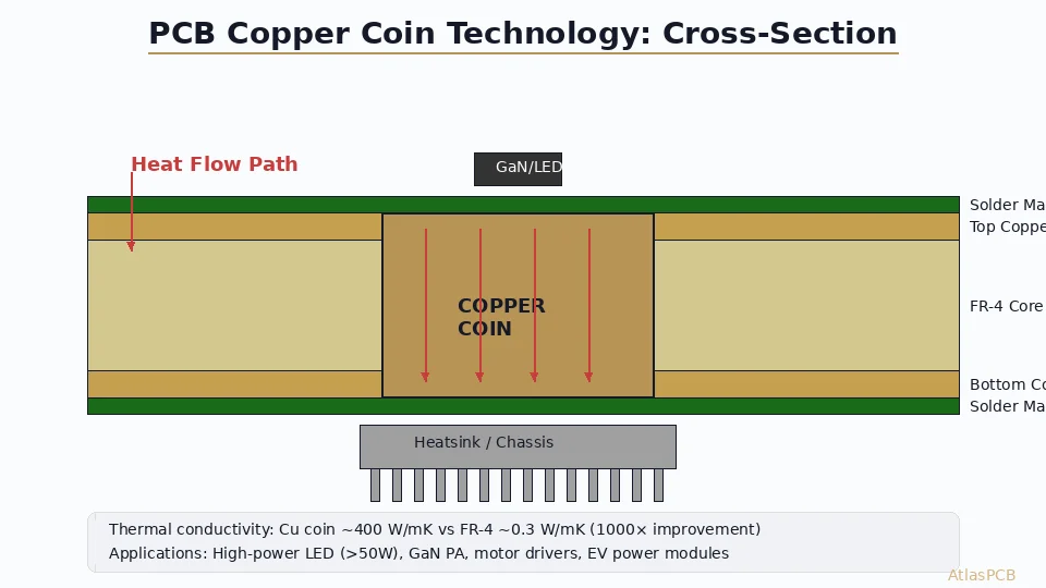
Copper coin technology solves this fundamental limitation by replacing the FR-4 dielectric directly beneath the heat source with solid copper, creating a thermal superhighway from junction to heatsink.
Copper Coin Technology Fundamentals
What Is a Copper Coin?
A copper coin is a precision-machined solid copper slug, typically made from C101 (OFHC - Oxygen-Free High Conductivity) copper, that is press-fit into a pre-routed cavity in the PCB during lamination. The coin spans the full board thickness (or partial thickness for embedded mid-layer coins), providing a continuous metallic thermal path.
Thermal Performance Comparison
| Thermal Path Method | Thermal Conductivity | Typical θ (junction-to-case) | Max Power |
|---|---|---|---|
| FR-4 only (1.6mm) | 0.3 W/m·K | 40-80 °C/W | <2W |
| Thermal via array (25 vias) | Effective 2-5 W/m·K | 5-15 °C/W | 5-20W |
| Copper coin (solid) | 400 W/m·K | 0.5-2 °C/W | 20-500W |
| Aluminum core (IMS) | 1-3 W/m·K substrate | 3-8 °C/W | 10-50W |
| Direct bonded copper (DBC) | 400 W/m·K Cu / 24 W/m·K AlN | 0.2-1 °C/W | 50-2000W |
The copper coin provides a ~1000× thermal conductivity improvement over FR-4 while maintaining the flexibility and routing density of a standard multi-layer PCB—something that aluminum-core (IMS) boards cannot offer due to their single or double-layer routing limitation.
Types of Copper Coin Implementation
Type 1: Full-thickness coin
- Coin spans entire PCB thickness
- Exposed on both top and bottom surfaces
- Provides lowest thermal resistance
- Requires component and heatsink on opposite sides
Type 2: Partial-thickness coin (blind coin)
- Coin recessed from one surface, flush with the other
- Allows routing over the coin on the recessed side
- Slightly higher thermal resistance than full-thickness
- More complex manufacturing
Type 3: Multi-layer embedded coin
- Coin embedded within inner layers
- Both surfaces available for component mounting
- Used in complex multi-chip modules
- Requires sequential lamination with coin insertion
Type 4: Stepped coin
- Coin with multiple diameter steps
- Upper portion matches component thermal pad
- Lower portion expands for heatsink contact area
- Optimizes both component attachment and heat spreading
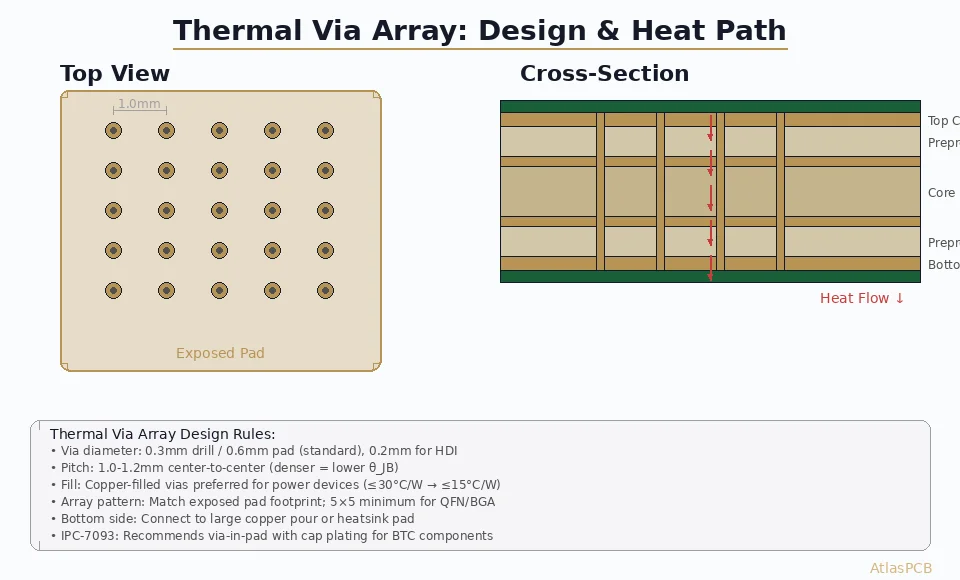
Design Rules and Guidelines
Coin Dimensional Specifications
Coin thickness: Must match the PCB stackup precisely. For a 1.6mm board with full-thickness coin:
- Target: 1.60mm ±0.05mm
- After plating: coin surface flush with outer copper layer ±25μm
Coin width/length: Determined by component thermal pad plus margin:
- Minimum coin size: component thermal pad + 0.5mm per side
- Maximum coin size: limited by routing/signal escape requirements around periphery
- Typical range: 5mm × 5mm to 30mm × 30mm
Cavity dimensions: Slightly larger than coin for press-fit:
- Cavity = Coin + 0.1mm per side (total 0.2mm clearance)
- Cavity corners: routed radius ≥0.5mm (matches router bit)
- Coin corners: chamfered or radiused to match cavity
Coin-to-trace clearance:
- Minimum 0.3mm from coin edge to nearest copper feature
- 0.5mm recommended for manufacturing margin
- Solder mask dam between coin and surrounding pads
Electrical Considerations
Copper coins are electrically conductive. This creates both opportunities and requirements:
Grounding: Most commonly, the coin is connected to ground plane(s). This provides excellent ground reference under the power component and reduces parasitic inductance.
Isolation: If the coin must be electrically floating (rare), apply a thin dielectric coating or maintain clearance on all layers. This significantly complicates manufacturing.
Plating: The coin surface receives the same surface finish as the rest of the board (ENIG, ENEPIG, HASL). Ensure finish compatibility with both component solder and heatsink attachment material.
PCB Layer Routing Around Coins
The coin creates a routing obstruction through all layers. Plan signal routing to avoid the coin area:
- Route critical signals around the coin periphery
- Use blind/buried vias for layer transitions near the coin
- Reserve at least 2-3 signal layers for routing that bypasses the coin zone
- Power planes can connect to the coin (if grounded) for additional heat spreading
Need Copper Coin PCB Manufacturing?
AtlasPCB manufactures copper coin embedded PCBs for LED lighting, RF power, and automotive power module applications with ±25μm flatness tolerance.
View Our Thermal PCB Capabilities →Manufacturing Process
Step-by-Step Fabrication
Step 1: Copper coin machining
- CNC milling from C101 copper bar stock
- Tolerances: ±0.05mm on thickness, ±0.1mm on width/length
- Surface finish: lapped to Ra <0.8μm for optimal bonding
- Cleaning: ultrasonic in acid bath to remove oxides
Step 2: Core preparation
- Route cavity in inner core layer using CNC routing
- Cavity depth matches coin insertion depth
- Cavity walls: straight or slightly tapered (0.5° draft)
- Clean cavity edges to remove burrs
Step 3: Coin insertion
- Press-fit coin into cavity with controlled force
- Alignment tolerance: ±0.1mm from design position
- Optional: apply thin layer of thermally conductive adhesive around perimeter
- Verify coin is flush with core surface (±25μm)
Step 4: Lamination
- Stack prepreg and outer layers over the coin area
- Modified press program: slower heat rate to account for copper mass
- Higher pressure may be required to ensure resin fills gaps around coin edges
- Post-lamination: verify no delamination or resin starvation near coin
Step 5: Drilling and plating
- Standard through-hole drilling avoids the coin area
- Vias adjacent to coin provide electrical connection if needed
- Copper plating builds up over coin surface to match outer copper thickness
Step 6: Surface preparation
- Planarize coin surface if necessary (belt sanding)
- Apply surface finish uniformly including coin area
- Solder mask applied with clearance window over coin thermal pad
Manufacturing Challenges
Challenge 1: CTE mismatch Copper CTE (~17 ppm/°C) differs from FR-4 CTE (~14 ppm/°C in-plane, ~50 ppm/°C z-axis). Solutions:
- Use high-Tg FR-4 (Tg >170°C) to minimize z-axis expansion
- Keep coin aspect ratio below 3:1 (length/thickness)
- Ensure adequate prepreg flow around coin perimeter to absorb stress
Challenge 2: Lamination pressure distribution The rigid copper coin doesn’t compress during lamination like prepreg. Solutions:
- Use conformal press pads (silicone) to distribute pressure
- Stepped coin profiles to reduce pressure differential
- Vacuum lamination to eliminate voids around coin edges
Challenge 3: Flatness after lamination Coin area may be slightly raised or depressed relative to board surface. Solutions:
- Target ±25μm flatness for solder printing
- Surface planarization by controlled belt grinding
- Alternative: use preformed solder or paste overprint for tolerance absorption
Application Examples
High-Power LED Arrays (30-200W)
LED arrays for stadium lighting, automotive headlamps, and UV curing require concentrated heat removal:
- Coin size: 15mm × 15mm to 25mm × 25mm
- Thermal budget: LED junction ≤ 85°C at ambient 55°C
- Calculation: For 50W LED on 20×20mm coin:
- θ_coin = L/(k×A) = 0.0016/(400×0.0004) = 0.01 °C/W
- Combined with thermal paste and heatsink: total θ ~2 °C/W
- Junction rise: 50W × 2°C/W = 100°C… requires larger coin or better heatsink
Optimization: increase coin to 30×30mm, use phase-change TIM, and aluminum fin heatsink for θ_total < 1.5°C/W.
GaN Power Amplifiers (10-100W RF)
GaN HEMT PAs in cellular base stations and radar systems:
- Extremely high power density: >5 W/mm gate periphery
- Coin placement: directly under GaN die attach area
- Additional requirement: ground return inductance through coin must be <0.1nH
- Coin connects to RF ground through multiple vias on perimeter
- Board material: often hybrid Rogers RF layers over FR-4 coin carrier
Automotive Motor Driver Modules (100-500W)
EV/HEV motor controllers using IGBT or SiC MOSFET modules:
- Multiple coins per board (one under each power device)
- Coin must withstand thermal cycling: -40°C to +150°C, 3000 cycles
- Vibration resistance: coin press-fit must survive 30g acceleration
- Automotive qualification: coin adhesion tested per IPC-TM-650
5G Massive MIMO Power Stages
Phased array antenna panels with distributed PAs:
- Array of small coins (5×5mm) under each PA element
- 64-256 coins per panel board
- Requires ultra-precise coin placement (±50μm) for antenna element alignment
- Lightweight copper alloy coins considered for weight-sensitive airborne arrays
Thermal Simulation and Verification
Finite Element Analysis (FEA)
Before committing to copper coin fabrication, validate thermal performance with FEA:
- Model the full stackup: component → solder → coin → TIM → heatsink
- Apply actual power dissipation from component datasheet
- Set boundary conditions: ambient temperature, airflow (natural or forced)
- Verify junction temperature stays within limits across operating range
- Check for thermal stress concentration at coin-PCB interface
Key Simulation Parameters
- Copper thermal conductivity: 400 W/m·K (use temperature-dependent values for precision)
- FR-4 thermal conductivity: 0.3 W/m·K (through-plane), 0.7 W/m·K (in-plane)
- Solder joint: 50 W/m·K (SAC305), typical 50μm thickness
- TIM: 1-5 W/m·K depending on type
- Contact resistance at coin-heatsink interface: include 20-50 mm²·K/W
Thermal Measurement Verification
After fabrication, verify thermal performance:
- Infrared (IR) camera imaging under power
- Thermocouple on coin surface (backside)
- Thermal test chip with embedded diode for accurate junction temperature
- Compare measured vs. simulated results; typical correlation within 10-15%
Cost Considerations
Copper coin PCBs typically cost 3-5× more than equivalent boards with thermal vias only:
| Cost Driver | Impact |
|---|---|
| CNC coin machining | 2-5 USD per coin depending on size |
| Cavity routing | +10-15% of board fabrication cost |
| Modified lamination | +20% processing time |
| Flatness inspection | Additional QC step |
| Yield loss | 5-10% coin insertion defects |
| Material (C101 copper) | 1-3 USD per coin material cost |
For a 100×100mm board with one 15×15mm coin, expect bare board cost increase of 30-50% over standard construction. At volumes above 1000 units, per-unit coin overhead drops significantly.
Design Checklist
Before submitting a copper coin design for fabrication:
- Coin size provides adequate margin over component thermal pad
- Cavity clearance: coin + 0.1mm per side
- Coin thickness matches stackup within ±0.05mm
- Electrical connection defined (ground or floating)
- Signal routing avoids coin footprint on all layers
- Solder mask opening defined over coin surface
- Surface finish compatible with solder attachment
- Flatness specification noted (±25μm for reflow)
- Thermal simulation validates junction temperature target
- Coin material specified (C101 OFHC standard)
- Assembly thermal profile accounts for copper mass
Further Reading
- PCB Thermal Via Array Design Rules
- PCB Design for GaN and SiC Power Devices
- PCB Thermal Management Fundamentals
- Heavy Copper PCB Manufacturing
Developing a high-power product that needs embedded copper thermal management? Our engineering team can review your thermal requirements and recommend the optimal copper coin configuration. Start a design consultation →
About AtlasPCB — We specialize in complex PCB manufacturing for HDI, RF, and high-reliability applications. Explore our heavy copper PCB manufacturing, or get an aluminum and metal-core PCB services . Every order includes free engineering review. Get your quote.
Reviewed by AtlasPCB Engineering Team — IPC-certified manufacturing specialists with 15+ years of production experience in HDI, RF, and high-reliability PCB fabrication. Content based on factory floor data and real customer design reviews.
- copper coin
- thermal management
- PCB
- power electronics
- high-power LED
- GaN
- embedded copper
- thermal conductivity
- heat dissipation