· AtlasPCB Engineering · Engineering · 10 min read
PCB Design for GaN and SiC Power Devices: Thermal Management, Layout Rules, and Material Selection
Complete guide to PCB design for gallium nitride (GaN) and silicon carbide (SiC) wide-bandgap power devices. Learn thermal via arrays, copper weight selection, creepage requirements, and high-frequency layout techniques for EV inverters, data center power, and industrial drives.

Introduction: Why Wide-Bandgap Devices Demand New PCB Design Rules
The power electronics industry is undergoing its most significant material transition in decades. Gallium nitride (GaN) and silicon carbide (SiC) wide-bandgap semiconductors are replacing silicon MOSFETs and IGBTs in applications ranging from EV inverters to data center power supplies — and they’re exposing PCB design limitations that never mattered with slower silicon devices.
Here’s the fundamental challenge: GaN devices switch at dV/dt rates of 50-200 V/ns and dI/dt rates of 5-20 A/ns. That’s 10-100× faster than conventional silicon IGBTs. At these speeds, every millimeter of PCB trace becomes a significant inductor, every copper plane becomes a transmission line, and thermal management becomes the primary factor limiting power density rather than the semiconductor’s electrical capability.
This guide covers everything you need to know about PCB design for GaN and SiC power devices: thermal management strategies that extract maximum performance, layout techniques that minimize parasitic inductance, material selection for high-voltage and high-temperature operation, and manufacturing considerations that ensure reliable production.
Understanding GaN vs. SiC: PCB Design Implications
Before diving into layout details, understanding the fundamental differences between GaN and SiC helps inform PCB design decisions:
GaN (Gallium Nitride)
- Typical voltages: 30-650V (commercially available), up to 900V emerging
- Switching speed: 2-10ns transitions, 1-5 MHz operation possible
- Package thermal pads: Bottom-side thermal pad (like QFN), requiring solder attachment to PCB
- Applications: Data center 48V-12V converters, EV on-board chargers, telecom rectifiers, motor drives <10kW
- PCB challenge: Extreme switching speed demands ultra-low inductance layout
SiC (Silicon Carbide)
- Typical voltages: 650-1700V, with 3300V devices available
- Switching speed: 10-50ns transitions, 50-200 kHz typical
- Package thermal pads: Top-side cooling (TO-247, D2PAK) or bottom-side (surface-mount modules)
- Applications: EV traction inverters, solar/wind converters, industrial drives >10kW, railway traction
- PCB challenge: High voltage demands generous creepage/clearance, heavy copper for high current
Both technologies share the requirement for excellent thermal management, but their different voltage/speed characteristics lead to distinct PCB design approaches.
Thermal Management: The #1 PCB Design Priority
For wide-bandgap power devices, the PCB isn’t just a circuit carrier — it’s the primary thermal path. Unlike TO-247 packages that bolt to external heatsinks, modern GaN devices in surface-mount packages rely entirely on the PCB to extract heat from the die.
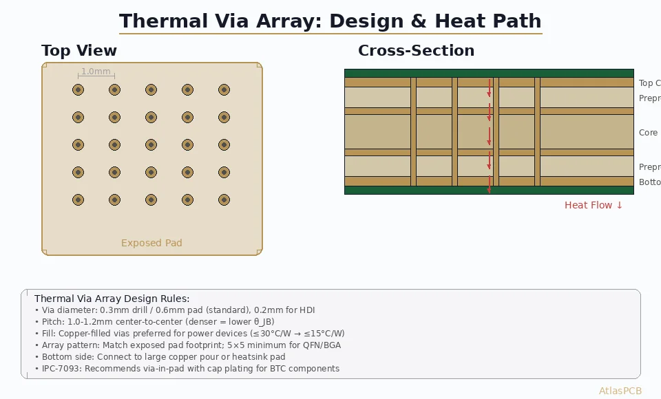
Thermal Via Array Design
The thermal via array beneath a power device is the most critical thermal feature on the board:
Design rules for thermal vias:
- Via diameter: 0.3mm (12mil) drill, 0.6mm (24mil) pad
- Via pitch: 1.0-1.2mm center-to-center (don’t go tighter — weakens the PCB)
- Fill method: Copper-filled and planarized (VIPPO process) for devices with exposed thermal pads
- Via type: Plated shut (filled) to prevent solder wicking during reflow
Why filled vias are mandatory for GaN:
Most GaN HEMTs (EPC, GaN Systems, Infineon CoolGaN) have a bottom-side exposed pad that serves as both the electrical drain/source connection and the thermal path. If vias beneath this pad are open (not filled), solder paste wicks down through the via barrel during reflow, creating:
- Void formation under the thermal pad (>25% voiding causes thermal failure)
- Reduced solder joint reliability
- Inconsistent electrical connection
Filled and capped vias with planarized surfaces ensure consistent solder paste printing and reflow results.
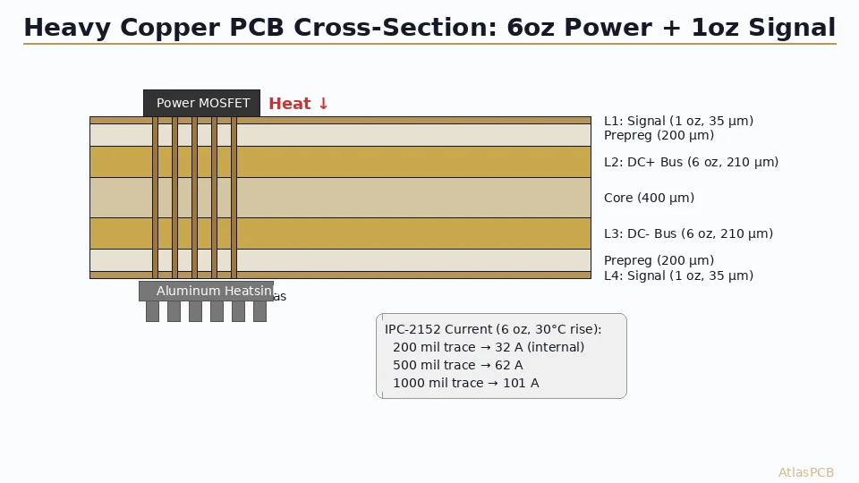
Copper Weight Selection
Heavy copper is essential for power device thermal spreading:
| Power Dissipation | Recommended Copper Weight | Stack-Up Strategy |
|---|---|---|
| <5W per device | 2oz outer, 1oz inner | Standard multilayer |
| 5-20W per device | 2oz outer, 2oz inner | Multiple ground/power planes |
| 20-50W per device | 3oz outer, 2-3oz inner | Dedicated thermal planes |
| >50W per device | 4oz outer + IMS/DBC | Metal-core or insulated metal substrate |
Important DFM consideration: Heavier copper reduces achievable trace resolution. Discuss your copper weight requirements with your PCB manufacturer during the design phase to understand minimum feature sizes.
Need Heavy Copper PCBs for Power Electronics?
AtlasPCB manufactures up to 6oz copper with thermal via fill — perfect for GaN and SiC applications
Get Your Power PCB Quote →Metal-Core and Insulated Metal Substrate (IMS) Options
When thermal via arrays alone cannot extract sufficient heat (typically above 50W per device or when board area is severely constrained), consider:
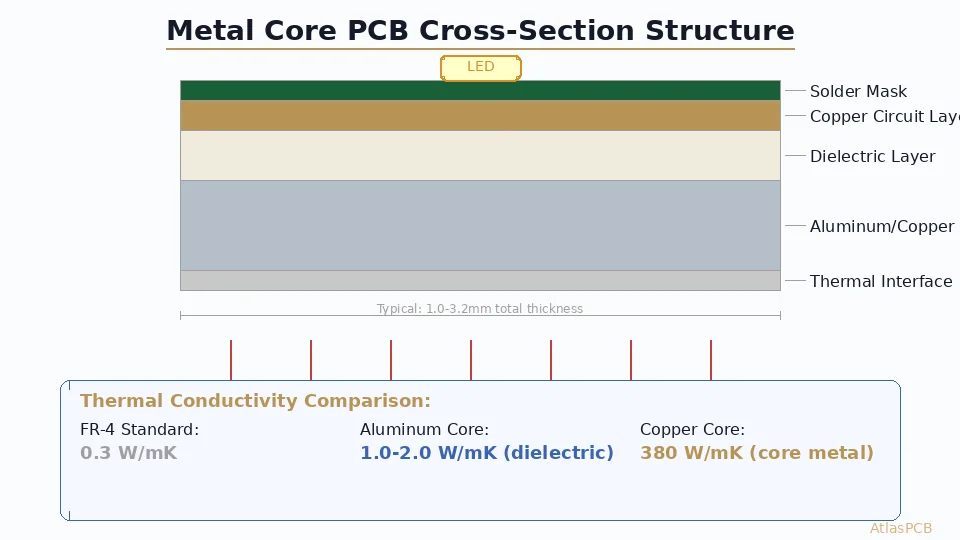
Insulated Metal Substrate (IMS):
- Aluminum or copper base (1.0-3.2mm thick)
- Thin dielectric layer (75-150µm) with thermal conductivity of 1-8 W/mK
- Single or double-sided copper circuit layer
- Best for: LED drivers, single-device power stages, simple topologies
Metal-core PCB (MCPCB):
- Aluminum or copper core laminated between standard FR-4 layers
- Allows multilayer construction while maintaining thermal path
- Thermal conductivity limited by dielectric: typically 1-3 W/mK
- Best for: Multi-device power stages requiring complex routing
Direct Bonded Copper (DBC) on Ceramic:
- Aluminum oxide (Al₂O₃) or aluminum nitride (AlN) ceramic substrate
- Copper directly bonded to ceramic (no adhesive)
- Exceptional thermal performance: 24-170 W/mK depending on ceramic
- Best for: High-reliability power modules, automotive-grade traction inverters
PCB Layout for Minimum Parasitic Inductance
Wide-bandgap devices switch so fast that PCB parasitic inductance — not the device’s RDS(on) — becomes the performance-limiting factor. Every nanohenry of loop inductance causes voltage overshoot during switching transitions, potentially destroying the device.
Power Loop Optimization
The power loop is the path current follows from the DC bus positive, through the high-side switch, through the low-side switch, and back through the DC bus capacitor. For minimum inductance:
Rule 1: Minimize loop area
Loop inductance is proportional to enclosed area. Place decoupling capacitors directly adjacent to the power device terminals — ideally within 2-3mm. Use low-ESL ceramic capacitors (0805 or 0603 size for minimum self-inductance).
Rule 2: Use adjacent-layer coupling
Route power loop current on adjacent copper layers separated by thin dielectric (4-5mil core). The mutual inductance between adjacent layers cancels loop inductance, achieving <0.5nH per cm of trace length versus 6-10nH/cm for single-layer microstrip.
Rule 3: Parallel current paths
Split the power loop across multiple parallel vias and traces. Six parallel 0.3mm vias have less inductance than a single 1.0mm via despite carrying the same current.
Gate Loop Optimization
The gate drive loop is equally critical — excessive gate loop inductance causes:
- Gate voltage ringing that can false-trigger the device
- Increased switching losses from delayed turn-on/turn-off
- EMI radiation from the high-dI/dt gate current
Target: <1nH total gate loop inductance
Achieve this by:
- Placing the gate driver IC within 5mm of the power device
- Routing gate and source-kelvin traces as a tightly coupled differential pair
- Using 0402 gate resistors to minimize trace length
- Connecting gate driver decoupling capacitors directly to the source kelvin pin
Layout Example: Half-Bridge GaN Stage
For a typical 400V/10A GaN half-bridge (e.g., EPC2206 or GaN Systems GS66508T):
- Layer 1 (Top): GaN devices, gate drivers, decoupling capacitors
- Layer 2 (Inner, 4mil below L1): Power return plane (bus negative)
- Layer 3 (Inner): Signal routing, gate drive traces
- Layer 4 (Inner): DC bus positive plane
- Layer 5 (Inner): Additional signal/thermal
- Layer 6 (Bottom): Thermal pad, heatsink attachment
The 4mil spacing between Layer 1 (device drain) and Layer 2 (bus negative) creates tight coupling that minimizes power loop inductance to approximately 0.3-0.5nH.
High-Voltage Design: Creepage and Clearance
SiC devices operating at 800V, 1200V, or even 1700V bus voltages impose strict isolation requirements on PCB layout:
IPC-2221B Requirements
| Working Voltage (DC) | Min. Clearance (sea level) | Min. Creepage (bare board) |
|---|---|---|
| 400V | 2.5mm | 4.0mm |
| 800V | 5.0mm | 8.0mm |
| 1200V | 8.0mm | 12.5mm |
| 1700V | 11.0mm | 17.0mm |
Critical note: These are bare-board minimums. Conformal coating reduces requirements, but high-altitude operation (avionics, drones) increases them significantly.
Design Strategies for High-Voltage Layouts
Slot/cutout isolation: Route milled slots in the PCB between high-voltage and low-voltage circuits. A 2mm slot provides equivalent isolation to approximately 8mm of surface creepage.
Controlled surface finish: ENIG or ENEPIG surface finishes maintain defined pad boundaries, preventing solder migration that could reduce effective clearances.
Solder mask integrity: Ensure solder mask coverage is continuous between high-voltage pads. Any solder mask void creates a contamination path that reduces effective creepage.
Buried vias for isolation: Use buried or blind vias to route signals beneath high-voltage areas without compromising surface creepage distances.
Material Selection for Wide-Bandgap Applications
Standard FR-4 works for many GaN applications below 200V and 200kHz, but higher-performance designs demand better materials:
Temperature Rating
GaN and SiC devices can operate at junction temperatures of 150-200°C. The PCB material must survive:
| Parameter | Standard FR-4 | High-Tg FR-4 | Polyimide | Ceramic-filled PTFE |
|---|---|---|---|---|
| Tg | 130-140°C | 170-180°C | 250°C+ | N/A |
| Td | 310-320°C | 340-360°C | 400°C+ | >400°C |
| Max operating | 105°C | 130°C | 200°C+ | 250°C+ |
| CTE (z-axis) | 60-70 ppm/°C | 40-50 ppm/°C | 35-45 ppm/°C | 24-30 ppm/°C |
For automotive-grade SiC inverters with 150°C ambient requirements, polyimide or ceramic-filled PTFE substrates are necessary.
Thermal Conductivity
Standard FR-4 has thermal conductivity of only 0.3 W/mK — essentially a thermal insulator. Better options:
- Metal-core substrates: 1-8 W/mK (depending on dielectric)
- Ceramic substrates: 24-170 W/mK (Al₂O₃ to AlN)
- Direct copper bonded: 170+ W/mK at the interface
High-Frequency Performance
At GaN switching frequencies (1-5 MHz), even power planes exhibit transmission-line behavior. For resonance-free power delivery:
- Low-Dk materials reduce parasitic capacitance in power planes
- Low-Df materials reduce high-frequency losses that cause heating
- Controlled Dk tolerance ensures predictable impedance
EMI Considerations in GaN PCB Design
The fast switching edges of GaN devices are prolific EMI generators. PCB design is the first line of defense:
Common-Mode Noise
Fast dV/dt across the switch couples through parasitic capacitances to the heatsink, chassis, and earth ground. Mitigation strategies:
- Faraday shield plane between power stage and sensitive circuits
- Guard rings around high-dV/dt nodes
- Minimized heatsink area under switching nodes (reduce parasitic capacitance to earth)
- Balanced layout so common-mode currents cancel in EMI filter inductors
Differential-Mode Noise
Fast dI/dt in power loops radiates magnetic fields. PCB mitigation:
- Adjacent-layer cancellation (as discussed in power loop section)
- Contained return paths — never force current to find its own return path
- Input filter placement close to the power stage, with ground plane continuity
- Shielded vias around sensitive analog circuits (current sensors, voltage dividers)
Manufacturing Considerations
Wide-bandgap power PCBs often require capabilities beyond standard PCB fabrication:
Thick Copper Processing
- Etch factor: 3oz+ copper requires wider trace spacing (minimum 10mil/10mil for 3oz)
- Drilling: Heavier copper increases drill wear; specify drill life limits with your manufacturer
- Plating uniformity: Thick copper makes uniform plating thickness harder; specify ±10% tolerance
Via Fill Quality
- Specify IPC-4761 Type VII (filled and capped) for thermal vias under power devices
- Dimple depth: ≤25µm maximum for proper solder paste printing
- Fill material: Copper fill provides best thermal performance; conductive epoxy fill is acceptable for thermal-only vias
Assembly Considerations
- Solder paste volume: Power device thermal pads need specific aperture ratios (70-80% of pad area)
- Reflow profile: Heavy copper boards need longer soak times due to higher thermal mass
- Void inspection: X-ray inspection of power device solder joints — target <25% voiding
- Clean assembly: Ionic contamination causes electrochemical migration at high voltages
Design Checklist for GaN/SiC PCBs
Before sending your design for manufacturing at AtlasPCB, verify:
- Thermal via array: minimum 0.3mm drill, 1.0-1.2mm pitch, filled and capped
- Copper weight: ≥2oz on power layers, discuss with fab house
- Power loop inductance: <2nH (use field solver or measure with VNA on prototype)
- Gate loop inductance: <1nH (gate driver within 5mm of device)
- Creepage/clearance per IPC-2221B for operating voltage
- Material Tg: ≥170°C for power applications
- Decoupling caps: low-ESL types within 3mm of power device
- Thermal simulation: confirms junction temperature within device ratings
- EMI shield plane between power stage and sensitive circuits
- Via-in-pad specification called out on fabrication drawing
Conclusion
Designing PCBs for GaN and SiC power devices requires rethinking conventional layout practices. The extreme switching speeds and power densities of wide-bandgap devices make PCB parasitic inductance and thermal resistance the primary performance limiters — not the semiconductor itself.
Success requires early collaboration between the circuit designer and PCB manufacturer. Stack-up selection, copper weight, via fill capability, and material choice all impact achievable performance and must be confirmed during the design phase rather than discovered during prototyping.
The transition to wide-bandgap power electronics is accelerating — driven by EV adoption, data center efficiency mandates, and renewable energy growth. Engineers who master PCB design for these devices will lead the next generation of power electronics innovation.
Ready to manufacture your GaN or SiC power PCB? Get a quote from AtlasPCB — we offer thick copper up to 6oz, filled thermal vias, and engineering review to optimize your power electronics design for manufacturing.
Further Reading
- [Aluminum PCB Thermal Design for High-Power LED and Motor Drivers: Material Selection, Stackup, and DFM Guide]/blog/aluminum-pcb-thermal-design-led-motor-driver/)
- [AI Hardware PCB Thermal Management: Advanced Multilayer Stackup Design for 1000W+ Processing Units]/blog/ai-hardware-pcb-thermal-management-multilayer-design/)
- [PCB Panelization and Array Design: V-Score vs Tab Routing, DFM Rules, and Cost Optimization]/blog/pcb-panelization-v-score-tab-routing-dfm-cost-optimization/)
- [mmWave PCB Material Selection: Rogers vs Megtron vs LCP for 5G and 6G Applications]/blog/mmwave-pcb-material-selection-rogers-megtron-lcp-5g-6g/)
- [Rogers PCB Fabrication: Material Sourcing, Lead Times & Quality Control]/blog/rogers-pcb-fabrication/)
- Material Options & Capabilities
About AtlasPCB — We specialize in complex PCB manufacturing for HDI, RF, and high-reliability applications. Explore our heavy copper PCB manufacturing, aluminum and metal-core PCB services, or get an free engineering DFM review . Every order includes free engineering review. Get your quote.
Reviewed by AtlasPCB Engineering Team — IPC-certified manufacturing specialists with 15+ years of production experience in HDI, RF, and high-reliability PCB fabrication. Content based on factory floor data and real customer design reviews.
- GaN PCB
- SiC PCB
- power electronics
- thermal management
- wide bandgap
- PCB layout
- EV inverter
- thermal vias
- DFM