· AtlasPCB Engineering · Engineering · 10 min read
PCB Thermal Via Arrays: Design Rules, Copper Fill, and Heat Dissipation for Power Electronics
Engineering guide to designing thermal via arrays for effective heat transfer in power PCBs — covering via diameter, pitch, fill options, array patterns, and thermal resistance calculations for QFN, BGA, and power module packages.

Power density in electronic systems continues to increase as designers pack more functionality into smaller footprints. Power converters, motor drivers, LED drivers, and processor modules all generate significant heat that must be conducted away from the active silicon through the PCB to an external heat sink or ambient air. Thermal via arrays are the primary mechanism for conducting heat through a PCB’s thickness, and their design directly determines whether a power device operates within safe junction temperature limits.
This guide covers the physics of thermal via heat transfer, practical design rules, copper fill options, and calculation methods for power electronics applications.
Why Thermal Vias Matter
In a typical power application, the thermal path from junction to ambient includes several thermal resistances in series:
θ_JA = θ_JC + θ_CS + θ_SB + θ_BA
Where:
- θ_JC = Junction to case (set by the IC package — designer cannot change this)
- θ_CS = Case to solder (determined by solder joint quality and exposed pad coverage)
- θ_SB = Solder to board (this is where thermal vias have the greatest impact)
- θ_BA = Board to ambient (determined by copper area, airflow, and heatsink)
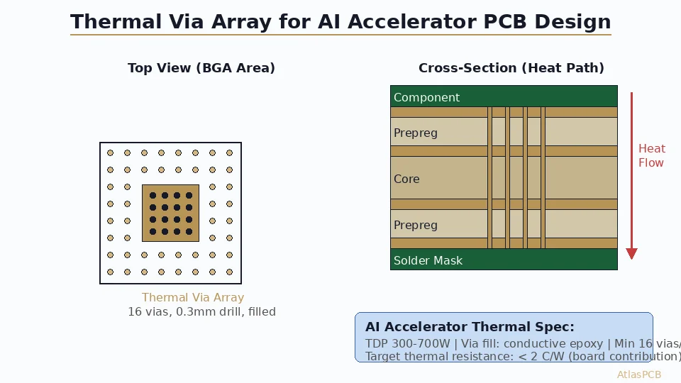
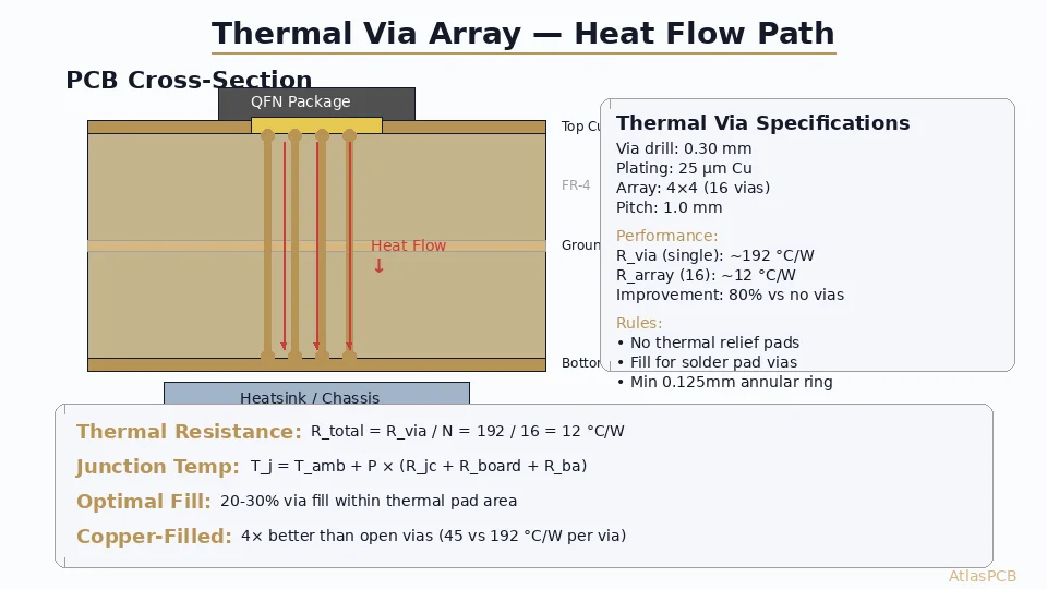
Without thermal vias, heat must spread laterally through the top copper layer — a path with high thermal resistance because copper traces are only 35–70 μm thick. A thermal via array provides a shortcut directly through the board’s thickness (typically 1.0–1.6mm), dramatically reducing θ_SB.
Quantitative impact: For a 1.6mm thick FR-4 board, the thermal conductivity through bare laminate is approximately 0.3 W/(m·K). A 0.3mm diameter copper-filled via has an effective thermal conductivity of approximately 380 W/(m·K) through its copper cross-section. Even accounting for the small via cross-sectional area, an array of 25 vias can reduce the effective through-board thermal resistance by 5–10×.
Thermal Via Design Parameters
Via Diameter
The via drill diameter directly determines the copper barrel cross-section and therefore the thermal conductance per via.
Standard thermal via: 0.3mm (12 mil) drill, 0.6mm (24 mil) pad
This is the most common choice for standard PCB fabrication. The 0.3mm drill can be through-plated on standard equipment with typical plating thickness of 20–25 μm on the barrel wall.
HDI thermal via: 0.15–0.2mm drill, laser drilled
Used in [HDI PCB designs]/blog/hdi-pcb-stackup-design-advanced/) where space is extremely limited. Smaller vias have less copper area per via but can be packed more densely. Laser-drilled microvias are typically limited to spanning one dielectric layer, so heat must transfer through multiple stacked or staggered microvias.
Large thermal via: 0.4–0.5mm drill
Used when maximum thermal conductance per via is needed and board space allows. Fewer large vias can sometimes be more cost-effective than many small vias, but be aware of solder wicking risks with larger barrel diameters.
Via Plating and Fill Options
The fill treatment of thermal vias has a profound impact on both thermal performance and assembly reliability:
1. Open (hollow) vias:
- Lowest cost — standard fabrication process
- Thermal conductance limited to the barrel wall (hollow center is an air gap)
- High risk of solder wicking during reflow assembly
- Must be tented or plugged on the component side to prevent solder loss
- Thermal resistance per via: approximately 50–80°C/W
2. Epoxy-filled and cap-plated:
- Moderate cost increase over open vias
- Epoxy fill prevents solder wicking
- Cap plating creates a flat pad surface for reliable soldering
- Epoxy has low thermal conductivity (~0.3 W/(m·K)) — thermal improvement is marginal over open vias
- Thermal resistance per via: approximately 40–60°C/W
3. Copper-filled and cap-plated:
- Highest cost — requires electroplating fill process
- Solid copper column provides maximum thermal conductance
- Best assembly reliability with flat, solderable surface
- Thermal resistance per via: approximately 15–30°C/W
- Recommended by IPC-7093 for high-power BTC packages
4. Conductive epoxy-filled:
- Moderate cost, better thermal performance than standard epoxy
- Silver-filled epoxy achieves ~3–5 W/(m·K) — roughly 10× better than standard epoxy
- Good compromise between cost and performance
- Thermal resistance per via: approximately 25–40°C/W
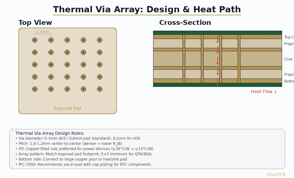
Via Pitch and Array Pattern
The via pitch (center-to-center spacing) determines how many vias fit within the exposed pad footprint:
- Standard pitch: 1.0–1.2mm — the most common choice, balances via count against board integrity
- Dense pitch: 0.8mm — used for high-power applications, requires quality control on drill alignment
- Maximum density: 0.65mm — approaching mechanical limits; board integrity may be compromised
Array patterns should match the exposed pad geometry:
- Square array (5×5, 6×6, etc.) — most common for square/rectangular exposed pads
- Staggered/hex array — provides ~15% more vias per unit area than square arrays
- Perimeter + fill — vias around the pad perimeter plus a filled center; ensures edge sealing for solder containment
A critical rule: via pads must not extend beyond the exposed pad boundary or they will interfere with the solder mask opening and potentially short to adjacent signal traces.
Thermal Resistance Calculations
The thermal resistance of a via array can be estimated using parallel resistance modeling:
Single via thermal resistance:
For an open (barrel-only) via:
R_via = L / (k_Cu × A_barrel)
A_barrel = π × (r_outer² - r_inner²)
Where:
- L = board thickness (e.g., 1.6mm)
- k_Cu = copper thermal conductivity (385 W/(m·K))
- r_outer = drill radius + plating thickness
- r_inner = drill radius
For a copper-filled via:
R_via = L / (k_Cu × π × r_outer²)Array thermal resistance (N vias in parallel):
R_array = R_via / NExample calculation:
25 copper-filled vias (0.3mm drill, 0.025mm plating), 1.6mm board:
r_outer = 0.175mm = 0.000175m
A_via = π × (0.000175)² = 9.62 × 10⁻⁸ m²
R_single = 0.0016 / (385 × 9.62 × 10⁻⁸) = 43.2°C/W
R_array = 43.2 / 25 = 1.73°C/W
This dramatically outperforms bare FR-4 (which would present ~85°C/W for the same pad area).

Need Copper-Filled Thermal Vias?
AtlasPCB offers copper-fill, epoxy-fill, and conductive-fill via options with DFM review to optimize your thermal design.
Get a Thermal PCB QuoteDesign Rules for Specific Package Types
QFN / DFN (Bottom-Terminated Components)
QFN packages are the most common application for thermal via arrays. The exposed metal pad on the bottom of the package is the primary thermal path.
Key rules:
- Match the via array to the QFN exposed pad dimensions
- Via pad diameter should be ≤50% of via pitch to maintain solder mask webbing
- Solder paste coverage on the exposed pad: 50–75% (windowed stencil pattern)
- Use via-in-pad with copper fill or dog-bone pattern with 0.2mm trace to offset via
- Bottom side: connect all vias to a large copper pour (minimum 2× the exposed pad area)
- IPC-7093 recommends minimum 9 vias for exposed pads ≤5mm × 5mm
BGA with Thermal Balls
Some BGA packages include dedicated thermal balls (usually in the center of the ball array) that require thermal vias underneath.
Key rules:
- Each thermal ball pad should have its own via or share vias with adjacent thermal balls
- Thermal ball vias must connect to internal ground/power planes for heat spreading
- Use the same [via-in-pad design rules as for signal BGA pads]/blog/bga-pad-design-via-in-pad-solder-voiding-prevention/)
- Consider blind vias if thermal balls are on a different grid than signal balls
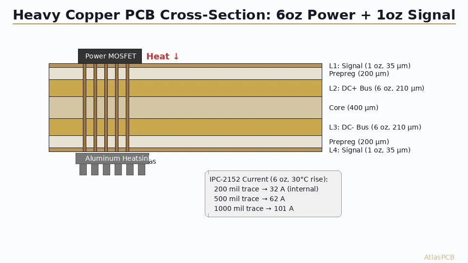
Power Modules (Half-Bridge, Full-Bridge)
Discrete power modules with exposed heatsink tabs dissipate 5–50W or more. These require aggressive thermal via strategies:
- Maximum via count within the heatsink tab area
- Copper-filled vias are strongly recommended (not optional)
- 2 oz or heavier copper on internal layers for lateral heat spreading
- Bottom-side copper area connected to chassis ground or heatsink
- Consider [thick copper PCB construction]/blog/pcb-copper-pour-ground-plane-design/) (3–4 oz) for extreme cases
- Thermal simulation is essential — hand calculations underestimate spreading resistance
LED Thermal Pads
High-power LEDs often use [aluminum-based PCBs]/blog/aluminum-pcb-thermal-design-led-motor-driver/) for thermal management, but when mounted on standard FR-4, thermal vias are the primary heat path.
Key rules:
- LED thermal pads are typically 3–5mm in diameter
- Use maximum via density (0.8mm pitch or tighter)
- Copper-filled vias are essential for high-power LEDs (>3W)
- Bottom-side pad should be soldered directly to a metal-core heat spreader
- Consider [hybrid stackup designs]/blog/pcb-thermal-management/) with aluminum or copper inlays
Board-Level Thermal Design Integration
Thermal vias are one component of a complete thermal management strategy. The following design elements work together:
Internal Plane Heat Spreading
Connect thermal vias to large copper areas on inner layers. The internal planes act as lateral heat spreaders, distributing the concentrated heat from the via array over a wider board area. Use continuous copper pours (no isolated thermal zones) connected to the via array on every possible layer.
Bottom-Side Copper Pour
The bottom-side copper pour directly under the thermal via array serves as the primary heat rejection surface. Design rules:
- Minimum area: 2× the via array footprint (4× preferred)
- No solder mask over the thermal copper (bare copper for heatsink contact)
- If a heatsink will be attached, include alignment features and thermal interface material (TIM) specifications in the assembly drawing
- Consider a ground via fence around the thermal area for [EMI containment]/blog/pcb-emi-shielding-via-fencing-board-level-shield/)
Thermal Relief Patterns
Thermal vias connected to ground or power planes need [thermal relief pads]/blog/pcb-thermal-relief-pad-design/) during assembly — but this creates a tradeoff. Thermal reliefs restrict heat flow.
For dedicated thermal vias (not carrying signal):
- Use direct connections (no thermal relief) to maximize heat transfer
- This makes hand soldering and rework more difficult but dramatically improves thermal performance
- If rework is a concern, use a 4-spoke thermal relief with 0.3mm spokes (wider than signal vias)
Common Design Mistakes
Mistake 1: Via pads extending beyond the exposed pad boundary This creates solder bridges to adjacent traces. Ensure all via pads are fully within the component pad mask opening.
Mistake 2: Too few vias because of concern about board weakening Structural integrity is rarely the limiting factor. A 5×5 array of 0.3mm vias in a 5mm pad represents only 3.5% of the pad area drilled out. The board can handle much more.
Mistake 3: Using standard solder paste stencil over via-in-pad Via-in-pad thermal arrays require windowed stencil patterns (50–75% coverage) to prevent excessive solder on the exposed pad, which can cause mid-chip solder balling or component floating during reflow.
Mistake 4: Ignoring solder wicking on open vias Open vias under thermal pads will drain solder during reflow, creating insufficient joints. Always use filled vias or dog-bone patterns for BTC packages.
Mistake 5: No bottom-side copper pour Without a bottom-side heat spreader, thermal vias have nowhere to dump their heat. The thermal resistance improvement is minimal without a continuous copper path to the final heat rejection surface.
Thermal Simulation vs. Calculation
Hand calculations (as shown above) provide useful first-order estimates but underestimate real-world thermal resistance because they ignore:
- Spreading resistance (heat must spread from a small via array to a larger copper area)
- Contact resistance between via barrel and internal copper layers
- Thermal interaction between adjacent vias (thermal shadowing)
- Convection and radiation from board surfaces
For designs where thermal margin is tight (junction temperature within 20°C of the maximum rating), use thermal simulation tools (ANSYS Icepak, Mentor FloTHERM, or free tools like Elmer FEM) to validate the design. The simulation should include:
- Actual copper coverage on each layer (from Gerber data)
- Via array geometry
- Component power dissipation maps
- Airflow conditions (natural convection or forced air)
- Heatsink thermal resistance (if present)
Conclusion
Thermal via array design is a quantitative engineering exercise that directly impacts product reliability. The key decisions — via diameter, fill type, pitch, and array size — should be driven by the thermal budget analysis for each power component on the board. Copper-filled vias provide the best thermal performance and are increasingly available from mainstream PCB fabricators at reasonable cost premiums.
For power electronics designs, invest the time in thermal simulation to validate your via array design before committing to fabrication. The cost of a thermal redesign far exceeds the engineering time for upfront simulation.
Designing a power PCB with demanding thermal requirements? AtlasPCB specializes in power electronics PCB fabrication with copper-filled vias, heavy copper (up to 6 oz), and aluminum-backed constructions. Request a DFM review and our thermal engineering team will optimize your via array design.
Further Reading
- [PCB Thermal Via Design Fundamentals]/blog/pcb-thermal-via-design/)
- [PCB Thermal Management: Strategies for High-Power Designs]/blog/pcb-thermal-management/)
- [Aluminum PCB Thermal Design for LED and Motor Drivers]/blog/aluminum-pcb-thermal-design-led-motor-driver/)
- [PCB Copper Pour and Ground Plane Design Best Practices]/blog/pcb-copper-pour-ground-plane-design/)
About AtlasPCB — We specialize in complex PCB manufacturing for HDI, RF, and high-reliability applications. Explore our HDI PCB manufacturing capabilities, heavy copper PCB manufacturing, or get an aluminum and metal-core PCB services . Every order includes free engineering review. Get your quote.
Reviewed by AtlasPCB Engineering Team — IPC-certified manufacturing specialists with 15+ years of production experience in HDI, RF, and high-reliability PCB fabrication. Content based on factory floor data and real customer design reviews.
- thermal via
- thermal management
- power electronics
- copper fill
- PCB design
- QFN
- heat dissipation
- via in pad