· AtlasPCB Engineering · Engineering · 9 min read
PCB DFM Check: The Complete Pre-Order Verification Guide for Engineers
Run a thorough PCB DFM check before ordering to avoid costly respins. This guide covers the critical design-for-manufacturability rules, common violations we catch, and how to verify your Gerber files are production-ready.
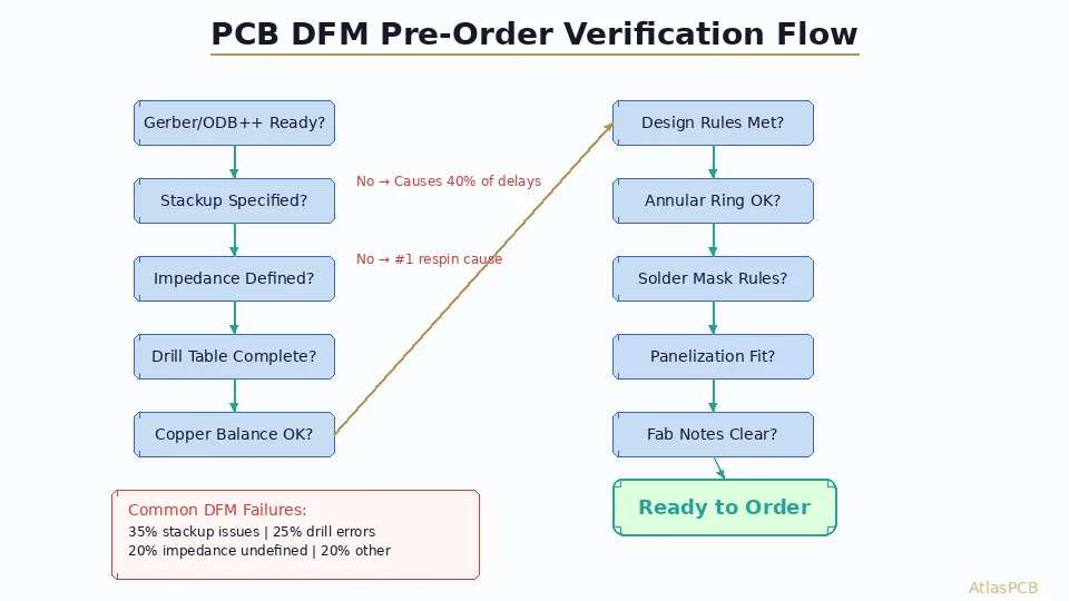
Quick Answer: The DFM Checklist That Catches 90% of Issues
Before submitting your Gerber files for fabrication, verify these critical parameters against your fabricator’s capabilities:
| DFM Parameter | Standard PCB | HDI PCB | Failure Mode if Violated |
|---|---|---|---|
| Min trace width | 4 mil (100um) | 3 mil (75um) | Open circuit, etching undercut |
| Min space | 4 mil (100um) | 3 mil (75um) | Short circuit, etch residue |
| Min annular ring | 4 mil (100um) | 2 mil (50um) | Breakout, unreliable via |
| Min drill (mech.) | 0.2mm | 0.15mm | Drill breakage, burr |
| Min drill (laser) | N/A | 0.075mm | Incomplete ablation |
| Drill-to-copper | 8 mil (200um) | 5 mil (125um) | Short to adjacent copper |
| Solder mask dam | 3 mil (75um) | 3 mil (75um) | Solder bridging between pads |
| Copper-to-edge | 10 mil (250um) | 8 mil (200um) | Copper exposure at routing |
| Aspect ratio (drill) | 10:1 | 0.8:1 (microvia) | Plating void, barrel crack |
If your design passes all parameters above against your chosen fabricator’s specs, you have eliminated the majority of manufacturing risk.
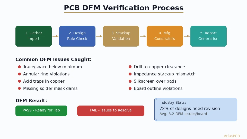
What a Professional DFM Check Actually Verifies
Most engineers think of DFM as simply running a design rule check (DRC) in their EDA tool. That catches the obvious — spacing violations, unrouted nets — but misses the manufacturing-specific constraints that cause real production failures. A proper DFM analysis goes substantially deeper.
Layer-by-Layer Copper Analysis
Your fabricator’s DFM team examines each copper layer for features that are technically “legal” per your design rules but problematic in real-world etching. Acid traps — acute-angle copper junctions below 90 degrees — create pockets where etchant cannot flow, leaving copper residue that causes shorts. Isolated copper features (thermal relief spokes, small isolated pads) can detach during the etching process if they lack adequate anchoring.
In our DFM review process, we flag approximately 8-12 acid traps per average 8-layer board. Most are in ground plane reliefs where the EDA auto-router created suboptimal thermal connections. These take 5 minutes to fix in the design but cause persistent yield issues if ignored.
Drill File Integrity
The drill file is where most silent DFM failures hide. Common issues we catch daily include: overlapping drill hits (two holes placed within 6 mil of each other, creating a slot instead of two holes), drill sizes not matching standard tooling (forcing tool changes that add cost), and drill hits placed closer to board edge than the routing tolerance allows.
One particularly insidious issue is non-plated holes (mounting holes, tooling holes) placed too close to copper features. Unlike plated through-holes which get copper deposition, NPTH holes are bare drilled — meaning any copper within 10 mil of the hole edge risks burr-induced shorting during the drilling operation.
ENGINEERING REVIEW INCLUDED
DFM Review on Every Order
We run automated and manual DFM analysis before production begins. Issues are flagged within 4 hours with specific fix recommendations — not just error codes.
Submit Your Design ›The Top 5 DFM Failures We See Every Week
Based on production data from our facility — processing 2000+ unique part numbers monthly — these are the DFM violations that most frequently require design revision or waiver:
1. Annular Ring Breakout (34% of all DFM flags)
The most common DFM failure is insufficient annular ring, particularly on vias placed near BGA breakout patterns. When a 0.3mm drill with 0.5mm pad is placed with typical fab tolerance of +/-2 mil registration, the effective annular ring drops from 4 mil nominal to 2 mil worst-case. If your design rule was set at 3 mil minimum annular ring, this via is marginal.
The fix: increase via pad size by 2 mil (1 mil per side) or reduce drill diameter. For 0.3mm vias, we recommend a minimum 0.55mm pad (0.125mm/5mil annular ring nominal) to provide adequate manufacturing margin.
2. Trace/Space Violations in BGA Breakout (28%)
Modern fine-pitch BGAs (0.5mm, 0.4mm pitch) force routing into tight geometries. A 0.5mm pitch BGA with dogbone vias requires 3/3 mil trace/space to break out two traces between pads — putting the design right at HDI capability limits. Standard fabrication (4/4 mil minimum) cannot produce this, yet we receive such designs regularly from engineers who didn’t verify their fabricator’s capabilities before routing.
The fix: confirm your fabricator supports 3/3 mil before beginning layout. If not, move to via-in-pad construction (eliminating the dogbone route-out entirely) or choose a higher layer count that provides escape routing on inner layers where pitch constraints are relaxed.
3. Missing Solder Mask Dams (18%)
Solder mask dams — the slivers of solder mask between adjacent SMD pads — prevent solder bridging during reflow assembly. The minimum reproducible dam width is 3 mil (75um) for most processes, with some advanced LDI (Laser Direct Imaging) capable of 2.5 mil. When fine-pitch QFP or connector pads are spaced such that the mask dam falls below minimum, the fabricator must either eliminate the dam entirely (risking solder bridges) or reject the design.
We see this most often on 0.4mm pitch QFP packages and fine-pitch connectors where the pad-to-pad gap is only 5-6 mil, leaving insufficient room for mask dam plus mask registration tolerance.
4. Impedance Stackup Incompatibility (12%)
Engineers specify impedance requirements (typically 50 ohm single-ended, 100 ohm differential) but design their trace widths based on theoretical stackup calculations that don’t match available laminate thicknesses. When the fabricator runs impedance simulation against real material data, the required trace width may differ by 1-2 mil from what’s in the design — requiring either a trace width deviation waiver or a redesign.
The fix: request your fabricator’s standard stackup options before beginning layout, and use their actual dielectric thickness and Dk values for impedance calculations. Most impedance-controlled PCB manufacturers will provide stackup recommendations with pre-calculated trace widths for standard impedance targets.
5. Copper Balance and Warp Risk (8%)
Boards with significantly asymmetric copper distribution — heavy copper fill on one side, sparse routing on the other — warp during lamination and reflow. While not always a DFM “violation,” our process engineers flag severe imbalance (>30% copper percentage difference between top/bottom) as a warp risk, recommending copper fill additions or thieving patterns to restore balance.
IMPEDANCE CONTROLLED PCB MANUFACTURER
Stackup Design Support Before You Route
Get impedance-optimized stackup recommendations with exact trace widths before layout begins. We provide layer-by-layer Dk values from real material data.
Request Stackup ›Running Your Own DFM Check: Tool-Specific Workflow
Altium Designer
Altium’s Design Rule Check (DRC) handles electrical and spacing validation well, but for manufacturing-specific DFM, use the “Fabrication Outputs” validation or export to ODB++ format (which carries more manufacturing context than Gerber). Set your design rules to match your fabricator’s capabilities:
- Routing → Width: Set minimum to fabricator’s min trace
- Routing → Clearance: Set minimum to fabricator’s min space
- Manufacturing → MinimumAnnularRing: Match fabricator spec
- Manufacturing → MinimumSolderMaskSliver: Set to 3 mil minimum
KiCad
KiCad 8.x includes improved DRC with manufacturing-oriented rules. Configure your custom rules file (.kicad_dru) with fabricator-specific constraints. Pay particular attention to the “via_annular_ring” and “silk_clearance” rules, which KiCad defaults conservatively but may not match your chosen process.
Cadence Allegro / OrCAD
Allegro’s constraint manager provides the most granular manufacturing rule control. Set “Physical” constraints under the Manufacturing category: Minimum Etch, Minimum Space, Minimum Pad-to-Pad, and Drill constraints. Run “Design Audit” before Gerber output to generate a comprehensive DFM report.
When to Skip DFM and When It Is Non-Negotiable
Acceptable to Relax DFM
- Personal hobby projects where yield loss is acceptable
- Quick-turn prototypes from budget services (they check for you, with wider margins)
- Simple 2-layer boards with 10/10 mil trace/space (far from capability limits)
DFM Is Critical
- Any board going to production volume (yield loss at scale is expensive)
- HDI PCB designs with features below 4/4 mil
- Impedance-controlled designs (stackup must be verified against real materials)
- Boards for regulated industries (medical, automotive, aerospace) where first-pass success is mandatory
- High layer count boards (8+ layers) where registration stack-up affects annular rings
- Flex and rigid-flex boards where bend zone DFM rules differ from rigid
FAST TURNAROUND
DFM Issues? We Fix Them — Not Just Flag Them
Our CAM team provides specific fix recommendations with annotated Gerber images, not just a list of error codes. Most DFM issues resolved same-day.
Get Quote + DFM Review ›Pre-Submission DFM Checklist
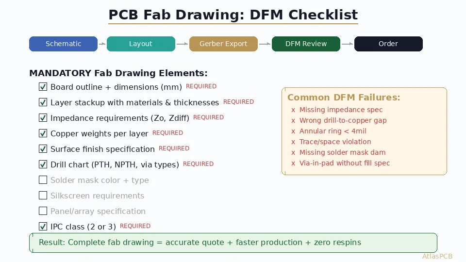
Before sending your Gerber files to any fabricator, verify:
| Check | How to Verify | Pass Criteria |
|---|---|---|
| Gerber file completeness | Open in viewer, count layers vs design | All layers present + drill file |
| Aperture list | Check D-code assignments | No zero-size apertures |
| Board outline | Verify closed contour | Single closed polygon, no gaps |
| Drill file format | Confirm Excellon 2 format | Coordinates match copper layers |
| Net connectivity | Run netlist vs. Gerber comparison | Zero opens, zero shorts |
| Layer stack order | Document in fab drawing or README | Unambiguous layer naming |
| Impedance notes | Include in fab drawing | Target Z, tolerance, reference layers |
| Special requirements | Surface finish, material, copper weight | Clearly specified |
A complete, unambiguous file package is the single most effective way to avoid DFM-related delays. We receive approximately 15% of orders with ambiguous layer assignments or missing drill files — each requiring a clarification cycle that adds 12-24 hours to lead time.
ATLASPCB
Submit Your Design — DFM Review Included
Every order includes comprehensive DFM analysis with engineering recommendations. Upload your Gerbers and get a detailed manufacturability report with your quote.
Upload Gerber Files ›Reviewed by AtlasPCB Engineering Team — 15+ years in advanced PCB fabrication for RF, HDI, and rigid-flex applications.
Related Reading:
About AtlasPCB — We specialize in complex PCB manufacturing for HDI, RF, and high-reliability applications. Explore our impedance-controlled PCB manufacturing, free engineering DFM review, or get an full PCB manufacturing capabilities . Every order includes free engineering review. Get your quote.
Reviewed by AtlasPCB Engineering Team — IPC-certified manufacturing specialists with 15+ years of production experience in HDI, RF, and high-reliability PCB fabrication. Content based on factory floor data and real customer design reviews.
- PCB DFM
- design for manufacturability
- Gerber files
- PCB manufacturing
- impedance controlled PCB