· AtlasPCB Engineering · Engineering · 9 min read
Ceramic PCB Technology: LTCC vs HTCC for High-Temperature and RF Applications
Complete guide to ceramic PCB substrate technology comparing Low-Temperature Co-fired Ceramics (LTCC) and High-Temperature Co-fired Ceramics (HTCC) — covering material properties, firing processes, conductor compatibility, thermal performance, and application selection for RF, aerospace, automotive, and power electronics.
Introduction: Why Ceramic Substrates for PCB Design?
Standard organic PCB substrates — FR-4, polyimide, Rogers PTFE — dominate 99% of electronics manufacturing. They’re inexpensive, well-characterized, and available from hundreds of fabricators worldwide.
But organic materials hit hard physical limits in extreme applications:
- Temperature ceiling: FR-4 glass transition (Tg) occurs at 130–180°C; polyimide extends to ~280°C; but many aerospace and automotive applications demand continuous operation at 300–500°C
- Hermeticity: Organic laminates absorb moisture (0.1–0.3% by weight), causing reliability failures in space, military, and medical implant applications
- RF losses: Even low-loss PTFE laminates exhibit Df > 0.001 at mmWave frequencies, limiting achievable Q-factors in filter and resonator designs
- CTE mismatch: Organic substrates (CTE 12–16 ppm/°C) create stress concentrations when bonded to silicon die (CTE 2.6 ppm/°C) or GaN/GaAs semiconductors (CTE 5–6 ppm/°C)
Ceramic PCB substrates solve all four problems simultaneously. Alumina (Al₂O₃) and glass-ceramic compositions provide:
- Operating temperatures exceeding 1000°C
- Zero moisture absorption (hermetic when sealed)
- Dielectric losses 10× lower than FR-4 at microwave frequencies
- CTE of 5–7 ppm/°C — closely matching semiconductor die materials
The tradeoff is cost: ceramic PCBs typically run 5–20× the price of equivalent organic boards, with longer lead times and fewer qualified manufacturers. This guide explains when the performance benefits justify ceramic technology and how to choose between LTCC and HTCC processes.
Ceramic PCB Material Systems
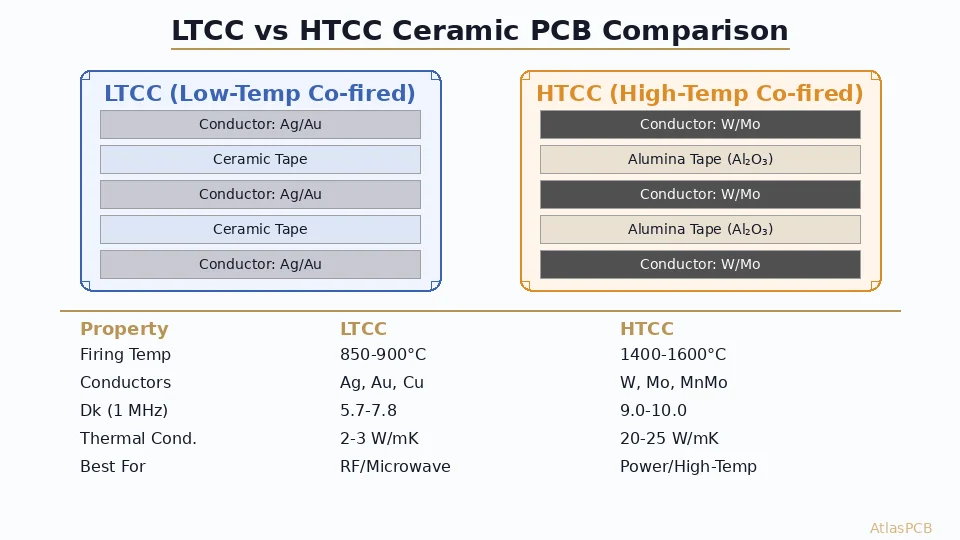
Alumina (Al₂O₃) — The HTCC Foundation
Pure alumina ceramics (96–99.6% Al₂O₃) represent the oldest and most proven ceramic substrate technology. Key properties:
| Property | 96% Alumina | 99.6% Alumina |
|---|---|---|
| Dielectric Constant (1 MHz) | 9.4 | 9.9 |
| Loss Tangent (1 MHz) | 0.0001 | 0.00003 |
| Thermal Conductivity | 24 W/mK | 35 W/mK |
| Flexural Strength | 350 MPa | 550 MPa |
| CTE (25–300°C) | 7.1 ppm/°C | 7.9 ppm/°C |
| Max Operating Temp | 1700°C | 1700°C |
Alumina’s exceptional thermal conductivity (80× better than FR-4) makes it the default choice for power electronics requiring efficient heat spreading. Its high dielectric constant (9–10) is a disadvantage for RF — signal wavelengths shrink, requiring tighter tolerances — but an advantage for miniaturization in non-RF applications.
Glass-Ceramics — The LTCC Foundation
LTCC tape systems use glass-ceramic compositions (typically a mixture of alumina, glass frit, and other oxides) with dielectric constants of 5.7–7.8. Leading material systems include:
- DuPont GreenTape 951 — Dk 7.8, Df 0.006 at 10 GHz, the industry workhorse
- DuPont GreenTape 9K7 — Dk 7.1, Df 0.001 at 10 GHz, ultra-low-loss for filters
- Ferro A6M — Dk 5.9, Df 0.002 at 10 GHz, matched to semiconductor die CTE
- Heraeus CT800 — Dk 7.5, Df 0.003, optimized for automotive radar at 77 GHz
The glass content enables sintering at 850–900°C — low enough for silver and gold co-firing — while maintaining mechanical integrity and hermeticity.
Aluminum Nitride (AlN) — Extreme Thermal Performance
For applications demanding maximum thermal dissipation, aluminum nitride substrates offer:
- Thermal conductivity: 170–230 W/mK (comparable to aluminum metal)
- CTE: 4.5 ppm/°C (excellent silicon die match)
- Dielectric constant: 8.8 at 1 MHz
AlN substrates are processed similarly to HTCC alumina but require nitrogen atmosphere sintering and specialized metallization (TiW/Ni/Au or direct-bond copper). Cost is 3–5× higher than alumina, justified for GaN power amplifiers, laser diode carriers, and high-power LED arrays.
LTCC Process Deep Dive
Manufacturing Steps
The LTCC fabrication sequence consists of seven stages:
Tape casting: Glass-ceramic slurry is cast onto a polymer carrier film, dried to form flexible “green” tape (50–250 μm per layer)
Via punching: Mechanical or laser punching creates via holes (minimum 75–100 μm diameter) through individual tape sheets
Via filling: Conductive paste (Ag, Au, or Ag/Pd) fills via holes using screen printing or vacuum techniques
Screen printing: Conductor patterns are printed onto tape surfaces using thick-film pastes — line widths down to 75 μm with specialized processes
Collation and lamination: Individual tape sheets are aligned, stacked, and laminated under pressure (20–30 MPa) at 70°C to form a monolithic green body
Co-firing: The laminated stack is fired in air at 850–900°C, simultaneously sintering the ceramic and metallization in a single thermal cycle
Post-fire processing: Optional steps include plating (Ni/Au over Ag), component attachment, and hermetic lid sealing
LTCC Conductor Options
| Metal | Resistivity (bulk) | Sheet Resistance | Solder Compatible | Migration Risk |
|---|---|---|---|---|
| Silver (Ag) | 1.6 μΩ·cm | 2–3 mΩ/□ | Yes (Ag-bearing) | High |
| Gold (Au) | 2.2 μΩ·cm | 3–5 mΩ/□ | Yes (Au-Sn) | None |
| Copper (Cu) | 1.7 μΩ·cm | 2–3 mΩ/□ | Yes (all) | Low |
| Ag/Pd (70/30) | 11 μΩ·cm | 10–15 mΩ/□ | Yes | Low |
Silver conductors dominate LTCC production due to lowest cost and best RF performance. Electromigration (silver migration) under DC bias with moisture present is managed through hermetic sealing and design rules (minimum 100 μm spacing at <50V).
Gold conductors eliminate migration risk entirely — mandatory for medical implants and long-life space applications despite 50× higher material cost.
Copper co-firing in LTCC requires nitrogen atmosphere (to prevent oxidation) and is offered by fewer fabricators, but enables lowest conductor losses and standard soldering compatibility.
Embedded Passives in LTCC
One of LTCC’s greatest advantages over HTCC and organic PCBs is the ability to embed passive components within the ceramic substrate:
- Capacitors: Parallel-plate structures using high-K dielectric pastes (εr 50–500) achieve 1 pF–100 nF in sub-mm² footprint
- Inductors: Spiral or helical conductor patterns provide 1–100 nH with Q-factors of 30–80 at GHz frequencies
- Resistors: Cermet paste compositions (RuO₂-based) provide 1 Ω–1 MΩ resistors with ±10% tolerance, trimmable to ±1% by laser
- Filters: Coupled-line and cavity resonator structures implement bandpass filters at 1–100 GHz entirely within the substrate
This integration eliminates hundreds of discrete components, reducing assembly cost, improving reliability, and shrinking module size by 50–80% compared to equivalent surface-mount designs.
HTCC Process Deep Dive
Manufacturing Steps
HTCC fabrication follows a similar sequence to LTCC but at dramatically higher temperatures:
Tape casting: High-purity alumina (96–99.6%) powder with organic binders forms green tapes (100–600 μm)
Via punching/filling: Via holes (minimum 100–150 μm) are filled with tungsten (W) or molybdenum (Mo) paste
Conductor printing: W or Mo paste is screen-printed for circuit patterns — minimum line width typically 100–125 μm
Lamination: Sheets are aligned and laminated at elevated pressure and temperature
Binder burnout: Slow thermal ramp (1–2°C/min) to 400–600°C removes organic binders
Co-firing: Sintering at 1400–1600°C in reducing atmosphere (H₂/N₂ mixed gas) to prevent tungsten oxidation
Post-metallization: Ni/Au plating over W/Mo pads for solderability and wire bonding
Why Refractory Metals?
At 1500°C, silver melts (961°C), gold melts (1064°C), and copper melts (1083°C). Only refractory metals survive HTCC firing temperatures:
- Tungsten (W): Melting point 3422°C, resistivity 5.3 μΩ·cm, good CTE match to alumina
- Molybdenum (Mo): Melting point 2623°C, resistivity 5.7 μΩ·cm, slightly better ductility than W
- Moly-Manganese (MoMn): Traditional metallization system for glass-sealed feedthroughs
The 3–4× higher resistivity of W/Mo versus Ag/Au means HTCC circuits have higher ohmic losses — a significant disadvantage for RF applications. However, HTCC’s thermal performance advantage (20–25 W/mK vs 2–3 W/mK for LTCC) makes it preferred for high-power dissipation requirements.
LTCC vs HTCC: Decision Matrix
Choose LTCC When:
- RF/microwave circuits are the primary function (filters, couplers, antenna arrays)
- Operating temperature is below 300°C
- Embedded passives reduce component count and assembly cost
- High Q-factor resonators or low insertion loss are critical
- 5G millimeter-wave front-end modules require sub-0.002 Df
- Size miniaturization through 3D integration is a priority
- Production volumes justify the tooling investment (>1000 units)
Choose HTCC When:
- Continuous operating temperature exceeds 300°C (downhole, jet engine, exhaust sensors)
- Maximum thermal dissipation is required (power amplifiers, laser carriers)
- Military/space applications demand proven heritage and qualification data
- Hermetic packaging with metal-to-ceramic brazed seals is necessary
- CTE matching to silicon requires the specific expansion characteristics of pure alumina
- Mechanical strength under vibration/shock loads is primary (flexural strength >350 MPa)
- Operating environment includes corrosive chemicals or radiation
Need Ceramic PCB Manufacturing?
AtlasPCB manufactures LTCC and HTCC ceramic substrates for RF, aerospace, and high-temperature applications — from prototypes to production volumes.
Application Examples
5G mmWave Front-End Module (LTCC)
A typical 28 GHz 5G antenna-in-package (AiP) module uses 10–20 layers of LTCC to integrate:
- Patch antenna array (4×4 or 8×8 elements)
- Beamforming network (phase shifters, power dividers)
- Bandpass filters (eliminating external SAW/BAW components)
- Transmission line interconnects to the RFIC
This level of integration in organic substrates would require multiple board-to-board connections, increasing losses and reducing reliability. LTCC’s consistent dielectric properties across all layers enable accurate filter tuning without post-fabrication trimming.
Automotive Exhaust Gas Sensor (HTCC)
Lambda (O₂) sensors in automotive exhaust systems operate at 300–900°C continuously. The sensor element is an HTCC alumina substrate with:
- Platinum sensing electrodes (fired after ceramic sintering)
- Embedded heater coil (W or Pt metallization)
- Gas diffusion barriers (porous ceramic layers)
- Hermetic lead-through connections to wiring harness
The ceramic substrate withstands millions of thermal cycles between ambient and 900°C — impossible with any organic PCB material.
Space-Grade DC-DC Converter Package (HTCC)
Radiation-hardened power converters for satellite applications use HTCC alumina packages providing:
- Hermetic cavity seal (brazed Kovar ring lid)
- Integrated heat spreader (AlN base plate)
- 50+ wire bond pads (Ni/Au over W metallization)
- Through-substrate vias connecting top circuits to bottom thermal slug
The hermetic seal prevents outgassing in vacuum and protects bond wires from atomic oxygen erosion in low-Earth orbit.
Design Rules and Manufacturability
LTCC Design Rules (Typical)
| Parameter | Standard | Advanced |
|---|---|---|
| Min line width | 100 μm | 50 μm |
| Min line spacing | 100 μm | 75 μm |
| Min via diameter | 150 μm | 75 μm |
| Via land diameter | 300 μm | 175 μm |
| Layer count | Up to 30 | Up to 50+ |
| Tape thickness | 50–250 μm | 25–100 μm |
| Fired shrinkage (X-Y) | 12.7% ±0.1% | Zero-shrink* |
| Positional accuracy | ±25 μm | ±10 μm |
*Zero-shrink LTCC (constrained sintering) uses sacrificial alumina layers to prevent X-Y shrinkage, achieving superior dimensional accuracy for fine-pitch packages.
HTCC Design Rules (Typical)
| Parameter | Standard | Advanced |
|---|---|---|
| Min line width | 125 μm | 75 μm |
| Min line spacing | 125 μm | 100 μm |
| Min via diameter | 150 μm | 100 μm |
| Via land diameter | 350 μm | 200 μm |
| Layer count | Up to 20 | Up to 40 |
| Tape thickness | 100–600 μm | 50–200 μm |
| Fired shrinkage (X-Y) | 16–20% ±0.3% | ±0.15% |
| Positional accuracy | ±50 μm | ±25 μm |
Common Design Pitfalls
Shrinkage prediction errors: Both LTCC and HTCC shrink during firing. Design dimensions must account for predictable shrinkage ratios — typically 12–20%. Component pads and via locations are scaled accordingly in design software.
Camber and warpage: Asymmetric metallization density between layers causes differential shrinkage, leading to substrate bowing. Balance conductor volume on top/bottom layers within 20%.
Via reliability at layer transitions: High aspect ratio vias (>5:1) in LTCC can crack during lamination or firing. Use staggered via arrays rather than stacked-via towers for thick substrates.
Thermal stress at joints: The rigid ceramic substrate does not flex — all thermal expansion mismatch with the PCB motherboard concentrates at solder joints. Use compliant (J-lead or gull-wing) rather than rigid (castellated) interconnections for large packages.
Cost Considerations
Ceramic PCB pricing depends on:
- Volume: NRE tooling ($5K–$50K) amortizes across production. Below 100 units, per-unit cost is dominated by tooling; above 10,000 units, material and processing drive cost.
- Layer count: Each additional layer adds ~15–25% to processing cost
- Metallization: Gold conductors add $30–$100/unit over silver for typical module sizes
- Inspection: 100% X-ray inspection for via fill quality and hermetic leak testing (He leak rate <10⁻⁸ atm·cc/s) add $5–$20/unit
- Typical pricing: Small LTCC module (15×15 mm, 8 layers) = $15–$40/unit at 1000 qty; HTCC package (25×25 mm, 4 layers) = $25–$80/unit at 1000 qty
Further Reading
- What Is Rogers PCB Material? — Compare ceramic with organic high-frequency laminates
- ENIG vs ENEPIG Surface Finish — Surface finish options compatible with ceramic substrates
- Embedded Component PCB Technology — Organic alternative to ceramic embedded passives
- Signal Integrity PCB Design Guide — High-frequency design principles applicable to ceramic substrates
Need ceramic PCB manufacturing for your RF module, sensor, or aerospace package? Contact AtlasPCB Engineering for LTCC and HTCC capabilities with MIL-spec qualification support.
About AtlasPCB — We specialize in complex PCB manufacturing for HDI, RF, and high-reliability applications. Explore our RF and high-frequency PCB services, or get an multilayer PCB fabrication up to 30 layers . Every order includes free engineering review. Get your quote.
Reviewed by AtlasPCB Engineering Team — IPC-certified manufacturing specialists with 15+ years of production experience in HDI, RF, and high-reliability PCB fabrication. Content based on factory floor data and real customer design reviews.
- ceramic PCB
- LTCC
- HTCC
- RF PCB
- high-temperature electronics
- alumina substrate
- multilayer ceramic
- aerospace PCB