· AtlasPCB Engineering · Engineering · 10 min read
PCB Copper Plating Uniformity: Throwing Power, Pattern Plating, and HDI Via Fill
In-depth guide to achieving uniform copper plating on PCBs — covering throwing power optimization, pattern vs panel plating trade-offs, pulse plating for HDI via fill, additive chemistry control, and IPC-6012 thickness requirements.
Introduction: The Foundation of PCB Reliability
Copper plating uniformity is arguably the single most critical factor in PCB manufacturing quality — yet it receives far less attention in design guides than routing rules or stackup optimization. Every electrical connection in a multilayer PCB depends on electroplated copper: the via walls that connect layers, the traces that carry signals, and the pads that anchor components.
When plating uniformity fails, the consequences cascade through the product lifecycle:
- Thin via walls create reliability time bombs that pass initial testing but fail under thermal cycling
- Uneven trace thickness causes impedance variations that corrupt high-speed signals
- Over-plated surfaces prevent fine-pitch component soldering
- Under-plated areas develop early copper fatigue cracks
This guide covers the physics, chemistry, and process engineering of achieving uniform copper plating — from the fundamental concept of throwing power through advanced pulse-plating techniques for [HDI microvia fill]/blog/hdi-pcb-technology/).
Throwing Power: The Core Metric
Definition and Physics
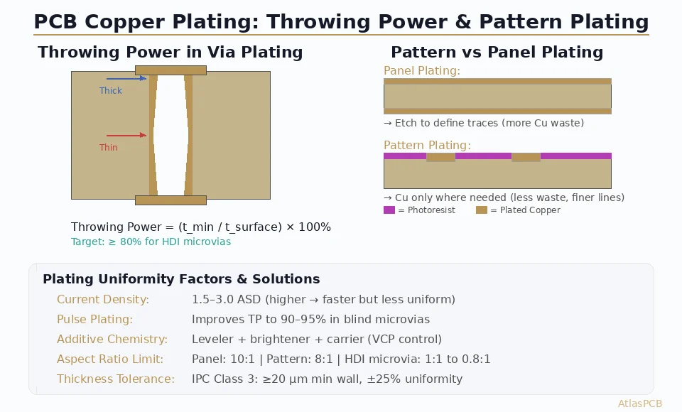
Throwing power quantifies how uniformly an electroplating bath distributes copper into recessed features compared to exposed surfaces. It’s defined as:
Throwing Power (%) = (t_min ÷ t_surface) × 100
Where:
- t_min = minimum copper thickness (typically at the center of a via hole wall)
- t_surface = copper thickness on the board surface near the via
The challenge is electrochemical: during plating, copper ions (Cu²⁺) must diffuse from the bulk electrolyte into confined spaces (via holes, narrow trenches). The surface — which is closer to the ion supply and has unobstructed current paths — always plates faster. The job of plating chemistry and process parameters is to minimize this difference.
Factors Affecting Throwing Power
Current density distribution: Faraday’s law dictates that copper deposits wherever current flows. Current follows the path of lowest resistance, which means edges, corners, and surfaces receive higher current density than hole interiors. At 2.0 ASD (amps per square decimeter) surface current, a 1.0 mm deep via might see only 0.8–1.2 ASD at its center.
Mass transport: Cu²⁺ ions deplete at fast-plating surfaces and must be replenished by diffusion and convection. Inside via holes, convection is limited — creating concentration gradients that slow deposition. Agitation (panel oscillation, solution flow, air sparging) partially mitigates this by driving fresh electrolyte into holes.
Additive chemistry: Modern acid copper plating baths use organic additives that dramatically modify deposition behavior:
- Suppressors (carriers): High-molecular-weight PEG/PPG polymers that adsorb on surfaces, locally increasing resistance and slowing plating. They accumulate on exposed surfaces more than in holes.
- Accelerators (brighteners): Small sulfur-containing molecules (SPS/MPS) that reduce overpotential and accelerate plating. They accumulate preferentially in recessed areas.
- Levelers: Nitrogen-containing compounds that adsorb at high-current-density points (edges, protrusions), locally suppressing deposition and smoothing the surface.
The interplay of these three additives creates “bottom-up” filling behavior — where recessed areas plate faster than surfaces — enabling void-free via fill.
Throwing Power Requirements by Application
| PCB Type | Via Aspect Ratio | Required TP | Typical Surface Cu |
|---|---|---|---|
| Standard multilayer | 6:1 to 8:1 | ≥60% | 25–35 µm |
| High-reliability (Class 3) | 8:1 to 10:1 | ≥75% | 30–40 µm |
| HDI (blind microvia) | 0.6:1 to 1:1 | ≥85% | 15–25 µm |
| HDI (via fill, no dimple) | 0.8:1 to 1.2:1 | ≥95% | 20–30 µm |
| Ultra-HDI (stacked via) | 1:1 to 1.5:1 | ≥90% | 15–20 µm |
Panel Plating vs Pattern Plating
Panel Plating Process
In panel plating, copper is electroplated across the entire board surface after drilling:
- Drill all through-holes and vias
- Electroless copper seed layer (0.5–1.0 µm) on all exposed surfaces including hole walls
- Electroplate copper across entire panel (typically 20–25 µm)
- Apply photoresist and image circuit pattern
- Etch away unwanted copper (subtractive process)
Advantages:
- Excellent plating uniformity (no pattern effects)
- Simple process with fewer steps before plating
- Higher throwing power (uniform current distribution)
- Better for thick copper requirements (≥2 oz)
Disadvantages:
- Limited minimum trace width (~75 µm due to etch undercut)
- Wastes copper (plates areas that are subsequently etched away)
- Higher etchant consumption
- Thicker surface copper makes impedance control harder
Pattern Plating Process
Pattern plating deposits copper selectively:
- Drill all through-holes and vias
- Electroless copper seed layer (0.5–1.0 µm)
- Thin flash electroplate (3–5 µm) for photoresist adhesion
- Apply photoresist and image (negative of circuit pattern — resist covers areas that should NOT be plated)
- Electroplate copper into open areas (traces, pads, hole walls) — typically 20–25 µm
- Electroplate etch resist (tin or tin-lead)
- Strip photoresist
- Etch base copper using etch resist as protection
- Strip etch resist
Advantages:
- Finer trace capability (50 µm lines achievable)
- Less copper waste (plates only circuit areas)
- Thinner base copper = less undercut during etch
- Better impedance control (more uniform final trace cross-section)
Disadvantages:
- Current crowding at resist edges causes thickness variation
- Dog-bone effect: traces near large copper areas plate thicker
- Via wall plating can be less uniform due to resist overhang
- More process steps = more opportunities for defects
The “Dog-Bone” Problem in Pattern Plating
Current crowding in pattern plating creates a characteristic problem: isolated traces (surrounded by resist) plate 20–40% thicker than traces adjacent to large copper areas (planes, pads). This happens because:
- Isolated traces have the entire surrounding electrolyte as their ion supply
- Traces near large copper areas must “share” ions with those areas
- The current density on an isolated fine trace can be 2–3× the nominal value
Solutions include:
- Thieving patterns: Non-functional copper features added to equalize current density across the panel
- Current robbing: Auxiliary cathodes or shield electrodes placed near panel edges
- Computational current distribution modeling: Optimizing resist pattern layout for uniform plating

Pulse and Pulse-Reverse Plating for HDI
Why DC Plating Falls Short for Via Fill
Conventional DC (direct current) plating achieves 60–70% throwing power in blind microvias with 1:1 aspect ratio. This means a via that requires 20 µm fill will accumulate 30+ µm on the surface — creating an unacceptable dimple or requiring extensive surface reduction (which risks damaging filled vias).
For [stacked microvia architectures]/blog/hdi-microvia-stacked-vs-staggered-reliability/) where each via must be filled completely flat (≤5 µm dimple) before the next layer is built, DC plating simply cannot achieve the required uniformity.
Pulse Plating (PP)
Pulse plating applies current in on/off cycles:
- T_on (forward pulse): 1–20 ms at 3–6 ASD (higher than DC average)
- T_off (rest period): 5–50 ms at 0 ASD
During T_off, ion concentration equalizes throughout the via — fresh Cu²⁺ diffuses into depleted areas. The next pulse then deposits more uniformly. Typical pulse plating achieves 75–85% throwing power.
Pulse-Reverse Plating (PRP)
Pulse-reverse adds a brief anodic (reverse) pulse:
- T_forward: 10–50 ms at 3–5 ASD (cathodic — depositing)
- T_reverse: 1–5 ms at 5–15 ASD (anodic — dissolving)
The reverse pulse preferentially dissolves copper from high-current-density points (via rim, surface protrusions) where the deposit is thickest. This levels the deposit from the top down while continuing to fill from the bottom up.
Results:
- Throwing power: 90–95%
- Dimple depth: ≤5 µm (meeting IPC-6012 via fill requirements)
- Void rate: <0.1% in microvias with ≤1:1 aspect ratio
HDI & ADVANCED PCB MANUFACTURING
Precision Copper Plating for HDI & Microvia Fill
AtlasPCB operates VCP plating lines with pulse-reverse capability, achieving ≥90% throwing power for stacked microvia architectures up to 1+N+1 HDI builds.
Get HDI PCB Quote →VCP (Vertical Continuous Plating) Lines
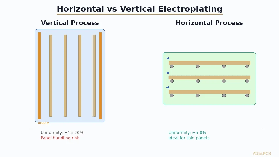
Modern Plating Line Architecture
High-volume PCB manufacturers have largely transitioned from horizontal rack plating to vertical continuous plating (VCP) systems. VCP lines offer:
- Continuous panel transport: Panels travel vertically through sequential tanks on carrier bars
- Consistent dwell time: Every panel receives identical plating time (no operator variation)
- Superior agitation: Combination of solution flow, panel oscillation, and eductor jets
- Real-time monitoring: Inline coulometry, thickness measurement, and additive dosing
A typical VCP line for PTH and via fill includes:
- Clean/microetch
- Acid dip
- Electroless copper (chemical deposition)
- Anti-tarnish
- Flash electroplate (3–5 µm DC)
- Main electroplate (15–25 µm, DC or pulse-reverse)
- Rinse cascade
Additive Control in VCP
VCP systems require precise additive maintenance because:
- Continuous plating consumes additives at a constant rate
- Organic additives break down under electrical current
- Temperature fluctuations affect additive activity
Control methods:
- CVS (Cyclic Voltammetric Stripping): Measures suppressor and accelerator activity
- HPLC (High-Performance Liquid Chromatography): Quantifies individual additive concentrations
- Hull cell testing: Quick visual check of deposit quality vs. current density
Most VCP lines now use automatic additive dosing based on coulombs consumed (amp-hours of plating), with CVS verification every 4–8 hours.
IPC Requirements for Plating Quality
IPC-6012 Minimum Copper Thickness
| Feature | Class 2 (Standard) | Class 3 (High-Reliability) |
|---|---|---|
| PTH wall (min) | 20 µm | 25 µm |
| Surface copper (min) | 20 µm | 25 µm |
| Via fill dimple (max) | — | ≤ 20 µm below surface |
| Via fill void | None penetrating ≥ 25% wall | None |
| Copper-to-copper (inner layer) | 1× foil thickness min | 1× foil thickness min |
IPC-6012 Annular Ring After Plating
For plated holes, the [annular ring]/blog/pcb-annular-ring-ipc-standards/) measurement includes both the base copper and the electroplated copper. Minimum annular ring after plating:
- Class 2: 50 µm (external), 25 µm (internal)
- Class 3: 50 µm (external and internal)
Cross-Section Analysis
Microsection (cross-section) analysis is the definitive quality verification for plating:
- Measure copper thickness at 3 points minimum on each hole wall (top, middle, bottom)
- Calculate throwing power from the measurements
- Verify no voids, cracks, or nodules in the deposit
- Check for resist intrusion or skip plating
For [via reliability testing]/blog/pcb-via-reliability-testing/), thermal stress tests (solder float at 288°C for 10 seconds) after plating verify that the copper grain structure can withstand manufacturing and field thermal cycles.
Practical Design Implications
For PCB Designers
Understanding plating uniformity helps you make better design decisions:
Avoid extreme aspect ratios: Design vias with aspect ratio ≤10:1 for standard PCBs, ≤1:1 for HDI microvias. Higher ratios require special plating processes that increase cost.
Balanced copper distribution: Uneven copper density causes plating non-uniformity. Use [copper thieving and balancing]/blog/pcb-copper-pour-ground-plane-design/) to equalize the platable area across your board.
Via-in-pad with fill: If using [via-in-pad]/blog/pcb-via-in-pad-plated-over-design/), specify “filled and planarized” in your fab notes. This triggers pulse-reverse plating + surface grinding.
Impedance impact: Plating adds copper thickness to traces. A 50 µm designed trace width with 25 µm plating on top becomes effectively taller by 25 µm — changing the impedance. Your [impedance calculation]/blog/pcb-impedance-control/) must account for plated copper thickness, not just base foil.
Minimum feature size vs. plating method: If you need traces <75 µm, you’re forcing your manufacturer into pattern plating (or mSAP/SAP processes). Understand the uniformity trade-offs.
For Procurement Engineers
When evaluating PCB manufacturers for plating quality:
- Ask for throwing power data from recent microsection reports
- Verify they have VCP (not rack) plating for consistency
- For HDI, confirm pulse-reverse plating capability
- Request CVS/HPLC additive control documentation
- Check IST (Interconnect Stress Test) results for via reliability
Advanced: mSAP and SAP Processes
For the most demanding applications (substrate-like PCBs, IC substrates), modified semi-additive (mSAP) and semi-additive (SAP) processes offer extreme fine-line capability:
mSAP: Start with ultra-thin copper foil (2–5 µm), pattern plate up to 15–20 µm, then etch the thin base copper. Achieves 30–50 µm lines/spaces.
SAP: No copper foil at all. Seed the dielectric surface with electroless copper (0.3–1.0 µm), pattern plate circuit features, then flash-etch the seed layer. Achieves 15–30 µm lines/spaces.
Both processes demand exceptional plating uniformity because the thin seed/base layer provides zero margin for over-etching. The plated copper IS the trace — there’s no thick base foil to provide a safety margin.
Troubleshooting Common Plating Issues
| Symptom | Root Cause | Solution |
|---|---|---|
| Thin spots on via walls | Low throwing power | Increase agitation, adjust additives, reduce current density |
| Nodules (bumps) on deposit | Contamination or additive imbalance | Carbon treat bath, replenish carrier |
| Rough/matte deposit | Excessive brightener or contamination | Reduce brightener dosage, check for organic breakdown |
| Via fill with center void | Premature surface seal | Increase leveler, use pulse-reverse |
| Dog-bone effect on traces | Current crowding in pattern plate | Add copper thieving, use shield electrodes |
| Burned deposit at edges | Excessive current density | Reduce current, add thieves at panel edges |
Further Reading
- [HDI PCB Technology Overview]/blog/hdi-pcb-technology/)
- [HDI Microvia Reliability: Stacked vs Staggered]/blog/hdi-microvia-stacked-vs-staggered-reliability/)
- [PCB Via-in-Pad Plated Over Design Guide]/blog/pcb-via-in-pad-plated-over-design/)
- [PCB Plating Void Prevention]/blog/pcb-plating-void-prevention/)
- [PCB Annular Ring IPC Standards]/blog/pcb-annular-ring-ipc-standards/)
Need PCBs with guaranteed plating quality? AtlasPCB provides microsection reports, throwing power verification, and IPC Class 3 plating for every HDI and high-reliability order. Get a quote or discuss your plating requirements with our engineering team.
About AtlasPCB — We specialize in complex PCB manufacturing for HDI, RF, and high-reliability applications. Explore our HDI PCB manufacturing capabilities, or get an full PCB manufacturing capabilities . Every order includes free engineering review. Get your quote.
Reviewed by AtlasPCB Engineering Team — IPC-certified manufacturing specialists with 15+ years of production experience in HDI, RF, and high-reliability PCB fabrication. Content based on factory floor data and real customer design reviews.
- copper plating
- throwing power
- pattern plating
- hdi
- via fill
- electroplating
- pcb manufacturing