· AtlasPCB Engineering · Engineering · 7 min read
TSMC CoWoS 11× Capacity Growth: How AI Packaging Demand Is Reshaping PCB Substrate Technology
Deep analysis of TSMC's 11× CoWoS capacity expansion and its cascading impact on PCB substrate technology—from ABF substrate shortages to glass-core innovations, 50μm design rules, and the convergence of IC packaging with PCB fabrication.
The Packaging Revolution Driving PCB Innovation
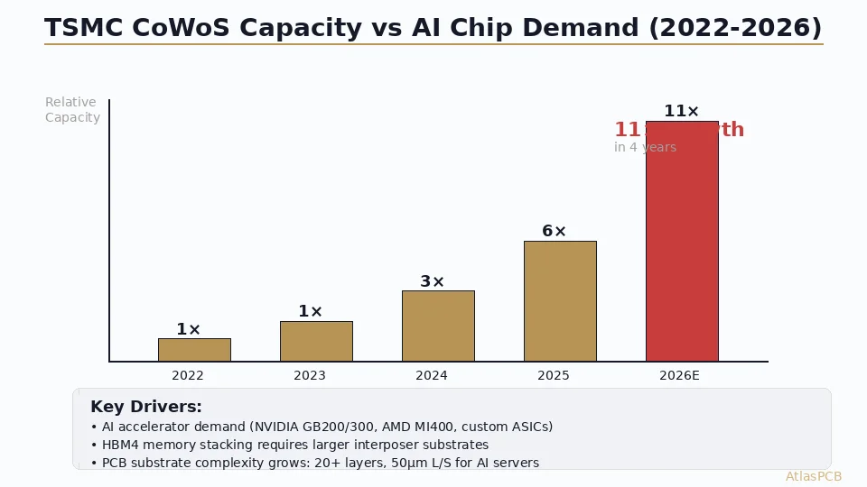
TSMC’s announcement of 11× AI accelerator wafer demand growth from 2022 to 2026 isn’t merely a semiconductor industry headline—it’s a fundamental technology inflection point for the entire PCB substrate ecosystem. The unprecedented scaling of CoWoS (Chip on Wafer on Substrate) advanced packaging is creating cascading demands that reshape how PCB substrates are designed, manufactured, and supplied.
The implications extend far beyond the handful of companies manufacturing CoWoS interposers directly. Every tier of the electronics supply chain—from laminate raw material suppliers to prototype PCB shops to high-volume motherboard fabricators—feels the pressure of AI packaging demand through material allocation, equipment availability, and shifting technical requirements.
This article examines the technical and supply chain implications of TSMC’s CoWoS expansion for PCB engineers, procurement teams, and fabrication facilities.
Understanding the 11× Demand Multiplier
To appreciate the magnitude, consider what 11× growth means in physical terms:
2022 baseline: TSMC’s CoWoS production primarily served NVIDIA A100/H100 and a handful of HPC/networking ASICs. Monthly CoWoS capacity: estimated ~15,000-20,000 wafer equivalents.
2026 projected: GB200/GB300 Superchips, AMD MI400, Google TPUv6, Amazon Trainium3, Microsoft Maia 200, and dozens of custom AI ASICs all requiring CoWoS or comparable packaging. Monthly capacity: ~165,000-220,000 wafer equivalents.
Each CoWoS package requires:
- One silicon interposer (65nm process, up to 2× reticle size via die-stitching)
- Multiple chiplets (2nm logic dies)
- 4-12 HBM memory stacks
- One organic package substrate (the PCB connection to the outside world)
The substrate for a single NVIDIA GB300 Superchip is approximately 100mm × 100mm—roughly 10× the area of a smartphone processor substrate.
PCB Substrate Technical Requirements for AI Packaging
Layer Count and Density
AI accelerator package substrates represent the most demanding PCB-like structures ever manufactured at scale:
| Parameter | Standard Server PCB | AI Accelerator Substrate | AI Server Motherboard |
|---|---|---|---|
| Layer count | 12-16 | 16-22 (redistribution) | 20-32 |
| Min trace/space | 75μm | 30-50μm | 50-75μm |
| Via technology | Mechanical drill | Laser microvia + core via | Sequential HDI |
| Materials | Standard Dk 3.8-4.2 | Ultra-low-loss Dk 3.0-3.3 | Low-loss Dk 3.3-3.6 |
| Panel size | 18×24” standard | 510×515mm or larger | 18×24” to 21×24” |
| Impedance tolerance | ±10% | ±5% | ±7% |
Material Demands
The substrate material hierarchy for AI packaging:
ABF (Ajinomoto Build-up Film): The workhorse for redistribution layers. Supply is critically constrained—Ajinomoto’s capacity expansion lags demand by 12-18 months.
Low-Dk core materials: Megtron 6/7 (Panasonic), Tachyon 100G (Isola), N4000-13 SI (Park). Used for signal-carrying cores where loss budget is critical.
Glass core (emerging): Intel, Samsung, and substrate makers are developing glass-core substrates with superior dimensional stability, thinner profiles, and better high-frequency performance. Expected volume production 2027-2028.
Silicon interposers: For the highest-density interconnect (5μm pitch), silicon bridges (Intel EMIB) or full-wafer interposers provide density impossible with organic substrates.
The Convergence of IC Substrates and PCBs
Building AI Hardware?
AtlasPCB fabricates high-layer-count HDI boards with sequential lamination, ultra-low-loss materials, and 50μm features for AI server evaluation platforms.
Get an AI Server PCB Quote →Perhaps the most significant long-term trend driven by CoWoS growth is the blurring boundary between IC packaging substrates and advanced PCBs:
From Substrates to Boards
Traditional distinction:
- IC substrate: Small (<80mm), many redistribution layers, 30μm features, ABF build-up
- PCB: Large (>200mm), fewer signal layers, 75μm+ features, FR-4 or low-loss laminate
Modern AI systems break this distinction:
- Substrates are growing to 100mm+, approaching board-scale dimensions
- PCBs are shrinking trace widths to 50μm, approaching substrate density
- Both use sequential lamination with microvia technology
- Both require ultra-low-loss dielectric materials
Manufacturing Process Crossover
Advanced PCB fabricators are adopting substrate-like processes:
- Modified semi-additive process (mSAP): Enables 30μm trace/space on organic PCBs
- Laser direct imaging (LDI): Replaces photo-tool exposure for fine features
- ABF-like build-up layers: Applied to PCB cores for smoother surfaces
- Panel-level processing: Substrate makers scaling to PCB-size panels for efficiency
Simultaneously, substrate manufacturers are scaling their infrastructure:
- Larger panel formats (from 340×340mm to 510×515mm)
- Higher throughput equipment (from IC substrate to mid-scale production)
- Diversified material systems beyond pure ABF
The net effect: a new category of “advanced interconnect” emerges that doesn’t fit neatly into either traditional PCB or traditional substrate classification. Companies positioned at this intersection—with both PCB-scale production capability and substrate-class process control—will capture the growing middle ground.
Design Rule Convergence
The practical convergence shows in design specifications:
| Design Rule | Traditional PCB | 2026 AI Server PCB | IC Substrate |
|---|---|---|---|
| Min trace width | 75-100μm | 50-75μm | 10-30μm |
| Min via drill | 150μm mechanical | 75μm laser | 25μm UV laser |
| Registration | ±50μm | ±25μm | ±10μm |
| Surface roughness | Ra 3-5μm | Ra 1-2μm | Ra <0.5μm |
| Layer count | 4-16 | 16-32 | 8-22 (redistribution) |
AI server PCBs now occupy the space between traditional PCBs and substrates, requiring hybrid manufacturing approaches.
Supply Chain Stress and Its PCB Industry Impact
ABF Substrate Shortage
Ajinomoto’s ABF production expansion timeline:
- 2024: ~30% capacity increase at Tosu factory
- 2025: Additional line at new Shizuoka facility
- 2026: Full ramp of Shizuoka + Thailand expansion announced
- Gap: Demand still exceeds supply by estimated 15-20% in 2026
This shortage cascades to PCB fabricators in several ways:
- Ultra-low-loss prepregs (sharing similar resin systems) see allocation constraints
- Equipment manufacturers prioritize substrate tool orders
- Laminate price increases of 20-40% year-over-year for premium materials
Workforce Competition
Substrate fabrication commands premium wages for process engineers. This creates talent migration from PCB shops:
- Process engineers with microvia experience recruited at 30-50% salary premiums
- Quality engineers with IPC-6016 (HDI substrate standard) knowledge in high demand
- R&D roles for glass-core substrate development attract advanced-degree candidates
Glass Core: The Next Frontier
Glass-core substrates represent the most significant substrate technology shift since ABF:
Advantages Over Organic Cores
- Dimensional stability: 3.3 ppm/°C CTE (vs 14-16 ppm for organic) closely matches silicon (2.6 ppm)
- Thickness reduction: Glass cores can be 100μm thin vs 400μm+ organic cores
- Electrical performance: Lower Dk (~5 for borosilicate, ~3.7 for modified glass) with excellent Df
- Via pitch: Through-glass vias (TGV) at 100μm pitch vs 300μm for mechanical drilling
- Surface smoothness: Ra <10nm enables fine-line RDL without planarization
Development Timeline
- 2024-2025: Intel, Samsung, AGC, Corning publishing research and prototyping
- 2026: Qualification samples and small-volume production for select customers
- 2027-2028: Expected volume production insertion for flagship AI accelerators
- 2029+: Potential displacement of organic core substrates for high-end applications
Implications for PCB Fabricators
Glass-core technology may eventually trickle down to advanced PCBs:
- Glass-reinforced high-performance laminates already use glass fibers
- TGV technology could enable finer via pitch in PCB cores
- Hybrid glass/organic stackups combining benefits of both materials
- New equipment requirements (TGV laser drilling, glass handling) represent significant investment
What PCB Engineers Should Do Now
Near-Term Actions (2026-2027)
- Qualify ultra-low-loss materials for AI server motherboard designs (Dk <3.5 at 10GHz)
- Adopt sequential lamination HDI for BGA breakout under AI processors
- Plan for larger panel sizes to efficiently manufacture large AI motherboards
- Back-drill capability for via stub removal on 112G+ channels
- Invest in LDI if pursuing sub-75μm features
- Secure material supply agreements for Megtron 6/7 and equivalent ultra-low-loss laminates before allocation constraints worsen
Medium-Term Preparation (2027-2029)
- Evaluate mSAP processes for achieving 30-50μm trace widths
- Monitor glass-core developments for potential adoption in high-end PCBs
- Develop hybrid stackup expertise (combining different material systems within one board)
- Scale impedance testing capacity for 100% verification on high-speed channels
- Recruit and train for substrate-class process control disciplines
- Establish partnerships with silicon interposer and advanced packaging suppliers to offer integrated solutions
Conclusion
TSMC’s 11× CoWoS growth isn’t just a number—it represents a fundamental remaking of the electronic interconnect landscape. The boundary between IC substrates and PCBs is dissolving, creating both challenges and opportunities for fabricators at every level. Those who invest in advanced capabilities now will be positioned to serve the insatiable demand for AI hardware interconnect in the coming decade.
The practical implications for PCB engineering teams are clear: master ultra-low-loss materials, develop sequential lamination HDI expertise, invest in fine-line imaging capability, and build relationships with material suppliers who can guarantee allocation during constrained periods. The AI infrastructure buildout is a multi-decade trend, and the interconnect complexity only grows from here.
For PCB fabricators serving the AI ecosystem, the competitive differentiation shifts from cost efficiency (a race to the bottom) to capability depth (process expertise, material qualification, yield at advanced design rules). Facilities that can deliver 20+ layer boards with 50μm features, controlled impedance on every pair, and ultra-low-loss materials at reasonable lead times will command premium pricing for years to come.
Further Reading
- T-Glass Shortage and AI Server PCB Demand
- TSMC CoWoS Advanced Packaging Capacity Report
- Sequential Lamination vs Build-Up HDI Process
- HDI PCB Stackup Design for Advanced Applications
Developing evaluation boards or production PCBs for AI server platforms? AtlasPCB’s sequential lamination HDI process supports up to 32 layers with 50μm features and ultra-low-loss materials. Request engineering consultation →
About AtlasPCB — We specialize in complex PCB manufacturing for HDI, RF, and high-reliability applications. Explore our HDI PCB manufacturing capabilities . Every order includes free engineering review. Get your quote.
Reviewed by AtlasPCB Engineering Team — IPC-certified manufacturing specialists with 15+ years of production experience in HDI, RF, and high-reliability PCB fabrication. Content based on factory floor data and real customer design reviews.
- AI
- PCB substrate
- CoWoS
- TSMC
- advanced packaging
- ABF
- glass core
- HDI
- HBM
- interposer