· AtlasPCB Engineering · Engineering · 8 min read
PCB Electrochemical Migration (ECM): Causes, Testing, and Prevention Strategies
Electrochemical migration causes dendritic shorts in humid environments. Learn how to prevent ECM failures through material selection, design rules, and IPC-compliant SIR testing.

Understanding Electrochemical Migration in PCBs
Electrochemical migration (ECM) remains one of the most insidious failure mechanisms in printed circuit boards. Unlike instantaneous failures that trigger immediate debug cycles, ECM develops gradually over weeks or months in the field — creating intermittent shorts that are nearly impossible to reproduce on the bench.
The mechanism is straightforward in principle but devastating in practice: when moisture condenses between two conductors at different electrical potentials, the higher-potential trace (anode) dissolves copper ions into the electrolyte. These Cu²⁺ ions migrate through the liquid film toward the lower-potential trace (cathode), where they reduce and deposit as metallic copper dendrites. Given enough time and persistent humidity, these dendrites bridge the gap completely, creating a hard short.
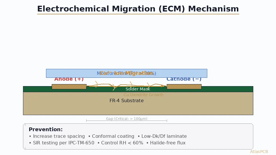
The electronics industry has seen ECM failures increase as trace geometries shrink below 100 μm pitch. What was a rare field failure in through-hole era designs has become a significant reliability concern for fine-pitch BGAs, 01005 passives, and HDI boards operating in uncontrolled environments.
The Three Requirements for ECM
ECM requires three simultaneous conditions. Remove any one, and the mechanism stops:
1. Moisture (Electrolyte)
The liquid film bridging two conductors serves as the electrolyte enabling ion transport. Sources include:
- Condensation — boards cycling through dew point in outdoor or industrial environments
- Hygroscopic flux residues — activator residues that absorb atmospheric moisture
- Process contamination — inadequate cleaning leaving ionic species on the surface
- Operating environment — sustained relative humidity above 60-80%
Even in “sealed” enclosures, thermal cycling creates condensation on PCB surfaces. A 10°C temperature drop in air at 70% RH pushes past dew point locally.
2. Ionic Contamination
The electrolyte’s conductivity depends on dissolved ions. Common sources:
- Flux residues — chloride and bromide activators are particularly aggressive
- Bare board contamination — etching chemicals, plating bath carryover
- Handling residues — fingerprints contain NaCl and organic acids
- Environmental pollutants — sulfur compounds, NOₓ in industrial atmospheres
IPC-J-STD-001 specifies maximum ionic contamination levels of 1.56 μg/cm² NaCl equivalent for Class 3 assemblies. Real-world failures often trace back to localized contamination exceeding this threshold.
3. Electrical Potential
A DC bias between adjacent conductors provides the driving force for anodic dissolution. The migration rate increases with:
- Higher voltage differential
- Continuous DC bias (worse than AC, which partially reverses dendrite growth)
- Fine-pitch geometries (shorter migration distance)
Surprisingly, even low voltages (3.3V logic) can drive ECM in contaminated, humid conditions. The critical factor is time — dendrites grow slowly at low bias but relentlessly.
Materials Most Susceptible to ECM
Not all metals migrate equally. Susceptibility ranking (most to least):
- Silver (Ag) — highest migration rate; problematic in silver-loaded epoxies and immersion silver finish
- Copper (Cu) — primary concern for PCB traces
- Tin (Sn) — relevant for solder joints and HASL finish
- Lead (Pb) — legacy concern for SnPb solder
- Gold (Au) — extremely resistant; one reason ENIG is preferred for high-reliability
Silver migration deserves special attention. Immersion silver (ImAg) surface finish, while excellent for solderability, creates ECM risk if the silver layer is exposed between pads. The industry has seen field failures in automotive modules where ImAg-finished boards operated in under-hood humidity without conformal coating.
Design Rules for ECM Prevention
Spacing Requirements
The fundamental defense is adequate conductor separation:
| Application Class | Min Spacing | Voltage Range | Environment |
|---|---|---|---|
| IPC Class 1 (consumer) | 80 μm | ≤50V DC | Indoor, controlled |
| IPC Class 2 (industrial) | 100 μm | ≤50V DC | Indoor, moderate |
| IPC Class 3 (high-rel) | 200 μm | ≤50V DC | Uncontrolled |
| High voltage (any class) | Per IPC-2221B tables | >50V DC | Any |
| Automotive (AEC-Q100) | 200+ μm | ≤16V DC | Under-hood |
For high-density interconnect boards operating at fine pitch, achieving these spacings while maintaining routing density requires careful stackup design and potentially adding routing layers.
Solder Mask Design
Solder mask is your first barrier against moisture films:
- Full mask coverage between adjacent conductors — no exposed FR-4
- Solder mask defined (SMD) pads for fine-pitch components reduce exposed copper
- Mask dam width ≥75 μm between pads (manufacturability limit ~50 μm for LPI)
- Adequate mask adhesion — delaminated mask creates capillary channels
Layout Strategies
- Route high-voltage and low-voltage traces on different layers where possible
- Avoid running traces parallel at minimum spacing for extended distances
- Place guard rings (grounded copper) around sensitive high-impedance nodes
- Orient traces so any potential dendrite growth direction does not create worst-case shorts

Need High-Reliability PCBs That Resist ECM?
AtlasPCB manufactures boards with controlled ionic contamination, SIR-validated processes, and conformal coating compatibility for automotive, medical, and aerospace applications.
Request a Quote →Manufacturing Process Controls
Flux Selection and Cleaning
The choice of flux chemistry directly impacts ECM risk:
- No-clean flux — low-residue formulations with benign activators. Still requires validation that residues pass SIR testing in the target humidity environment
- Water-soluble flux — aggressive activators that MUST be completely removed. Requires validated aqueous cleaning with conductivity monitoring
- Rosin-based flux — traditional, relatively safe residues when properly cured. Encapsulated activators reduce ion availability
For Class 3 assemblies, specify halide-free flux (IPC J-STD-004B classification: ROL0 or REL0) and verify post-clean ionic contamination with ROSE (Resistivity of Solvent Extract) or ion chromatography testing.
Laminate Quality
The base FR-4 material contributes to ECM susceptibility through:
- Conductive Anodic Filament (CAF) formation along glass fiber/resin interfaces
- Hollow fibers wicking moisture into the substrate
- Resin cure state — under-cured resin has higher moisture absorption
For reliability-critical designs, specify CAF-resistant laminates with:
- Spread glass (flattened weave reducing capillary paths)
- Modified resin systems with enhanced glass-resin adhesion
- Tg > 170°C (indicating full cure and lower moisture absorption)
Learn more about CAF resistance in PCB design for detailed laminate selection guidance.
Process Contamination Control
Manufacturing contamination must be controlled at every step:
- Bare board cleanliness — ionic contamination testing per IPC-TM-650 Method 2.3.25
- Storage conditions — vacuum-sealed with desiccant; exposure limits per J-STD-033
- Handling — gloves, ESD-safe workstations, controlled environment
- Solder paste — verify paste flux compatibility with SIR requirements
Testing and Validation
Surface Insulation Resistance (SIR) Testing
SIR testing per IPC-TM-650 Method 2.6.3.7 is the gold standard for ECM susceptibility assessment:
Test Conditions:
- Temperature: 85°C
- Relative Humidity: 85%
- Bias: 10–100V DC (typically 50V for standard testing)
- Duration: 500 hours minimum (168 hours for screening)
- Pass criterion: SIR > 10⁸ Ω throughout test
Test Vehicle:
- IPC-B-25A or equivalent comb pattern
- Represents production conductor geometries
- Must use actual production materials and processes
Electromigration vs. Electrochemical Migration
These are distinct mechanisms often confused:
- Electromigration — solid-state atom transport at high current density (IC-level concern, not PCB-level at standard currents)
- Electrochemical migration — solution-phase ion transport requiring a liquid electrolyte (the PCB concern)
Accelerated Life Testing
Beyond SIR, accelerated testing protocols include:
- HAST (Highly Accelerated Stress Test) — 130°C/85% RH for shorter test times
- Temperature-humidity cycling — simulates field condensation cycles
- Powered HALT — combines thermal cycling with electrical bias
Conformal Coating as a Barrier
Conformal coating provides a moisture barrier over assembled PCBs:
Coating Types for ECM Prevention
| Coating Type | ECM Protection | Application | Rework |
|---|---|---|---|
| Acrylic (AR) | Good | Spray/dip | Easy |
| Silicone (SR) | Good | Spray | Moderate |
| Urethane (UR) | Excellent | Spray/selective | Difficult |
| Parylene (XY) | Excellent | CVD | Very difficult |
| Epoxy (ER) | Excellent | Spray/dip | Not reworkable |
Application considerations:
- Minimum 25 μm thickness for moisture barrier effectiveness
- 100% coverage verification (UV fluorescence for coatings with UV tracer)
- Edge coverage — coating tends to thin at sharp edges and vertical surfaces
- Connector and test point masking compatibility
Coating Limitations
Conformal coating is not a cure-all:
- Under-board moisture can migrate through vias
- Thermal cycling creates micro-cracks over time
- Non-wetted areas (under tall components) remain vulnerable
- Coating adhesion depends on surface cleanliness — contaminated surfaces defeat the purpose
Real-World Case Studies
Case 1: Automotive ECU Failure
An automotive ECU experienced intermittent communication failures after 18 months in Southeast Asian markets. Root cause: no-clean flux residues under a QFN package absorbed moisture during monsoon season, enabling ECM between adjacent signal traces at 3.3V. The 80 μm trace spacing was adequate for indoor environments but insufficient for under-hood thermal cycling creating condensation.
Fix: Increased spacing to 200 μm on critical nets, switched to water-soluble flux with validated cleaning, and added selective conformal coating.
Case 2: LED Driver Module
An LED driver operating at 48V DC experienced field failures in refrigerated display cases. The cyclic temperature environment created regular condensation. ECM grew dendrites across 150 μm gaps between high-side and low-side traces.
Fix: Redesigned with 400 μm spacing on 48V nets, specified CAF-resistant laminate, and applied urethane conformal coating rated for condensing environments.
IPC Standards Reference
Key standards governing ECM prevention:
- IPC-2221B — Generic Standard on Printed Board Design (spacing tables)
- IPC-TM-650 2.6.3.7 — Surface Insulation Resistance
- IPC-TM-650 2.3.25 — Ionic contamination (ROSE test)
- IPC-J-STD-001 — Requirements for Soldered Electrical and Electronic Assemblies
- IPC-9202 — Material and Process Characterization/Qualification Test Protocol for Assessing Electrochemical Performance
- IPC-9203 — Users Guide for IPC-9202
For deeper understanding of PCB reliability testing methods, including how SIR fits into broader qualification programs, see our dedicated testing guide.
Summary and Design Checklist
Preventing ECM requires a holistic approach spanning design, materials, manufacturing, and testing:
✅ Conductor spacing ≥ IPC minimums for target environment class
✅ Full solder mask coverage between conductors at different potentials
✅ CAF-resistant laminate for high-reliability applications
✅ Halide-free or properly cleaned flux residues
✅ Ionic contamination verified < 1.56 μg/cm² (Class 3)
✅ SIR testing validates production processes pass 85/85/500h
✅ Conformal coating where environmental conditions demand it
✅ Guard traces/rings around high-impedance, high-value nets
Further Reading
- PCB CAF Resistance Design Guide
- PCB Via Reliability Testing Methods
- HDI Microvia Reliability: Stacked vs Staggered
- PCB Copper Plating: Electroless vs Electrolytic for HDI Vias
- Controlled Impedance PCB Stackup Design Rules
Designing boards for harsh environments? AtlasPCB provides IPC Class 3 manufacturing with validated SIR processes, CAF-resistant materials, and conformal coating compatibility. Get a free DFM review →
About AtlasPCB — We specialize in complex PCB manufacturing for HDI, RF, and high-reliability applications. Explore our full PCB manufacturing capabilities, or get an impedance-controlled PCB manufacturing . Every order includes free engineering review. Get your quote.
Reviewed by AtlasPCB Engineering Team — IPC-certified manufacturing specialists with 15+ years of production experience in HDI, RF, and high-reliability PCB fabrication. Content based on factory floor data and real customer design reviews.
- pcb-reliability
- electrochemical-migration
- manufacturing
- ipc-standards
- conformal-coating