· AtlasPCB Engineering · Engineering · 13 min read
Controlled-Depth Drilling in PCBs Explained
Master controlled-depth drilling for back-drilling, blind vias, and depth-controlled routing in high-speed PCB designs.
Introduction: Why Depth Matters in Modern PCB Drilling
As serial data rates push past 10 Gbps, 25 Gbps, and into 56 Gbps territory, the interconnect—not just the silicon—becomes the performance bottleneck. Via stubs, excess copper barrels, and poorly formed blind vias introduce impedance discontinuities, resonant cavities, and mode conversion that cripple channel margins. Controlled-depth drilling addresses these problems at the fabrication level by allowing the drill to stop at a precise point within the PCB stackup.
Controlled-depth drilling is not a single technique but a family of processes: back-drilling (removing via stubs after lamination), blind via drilling (forming vias that connect an outer layer to a specific inner layer), and depth-controlled routing (milling cavities, channels, or pockets to exact depths). Each process shares common machine capabilities—z-axis depth sensing, spindle speed control, and hit-count management—but applies them to different design requirements.
This guide covers the physics behind why controlled depth matters, the fabrication processes involved, design rules and tolerances, and practical guidance for specifying controlled-depth drilling in your next [high-speed PCB design]/blog/high-speed-pcb-design/).
The Physics of Via Stubs and Resonance
Quarter-Wave Resonance in Via Stubs
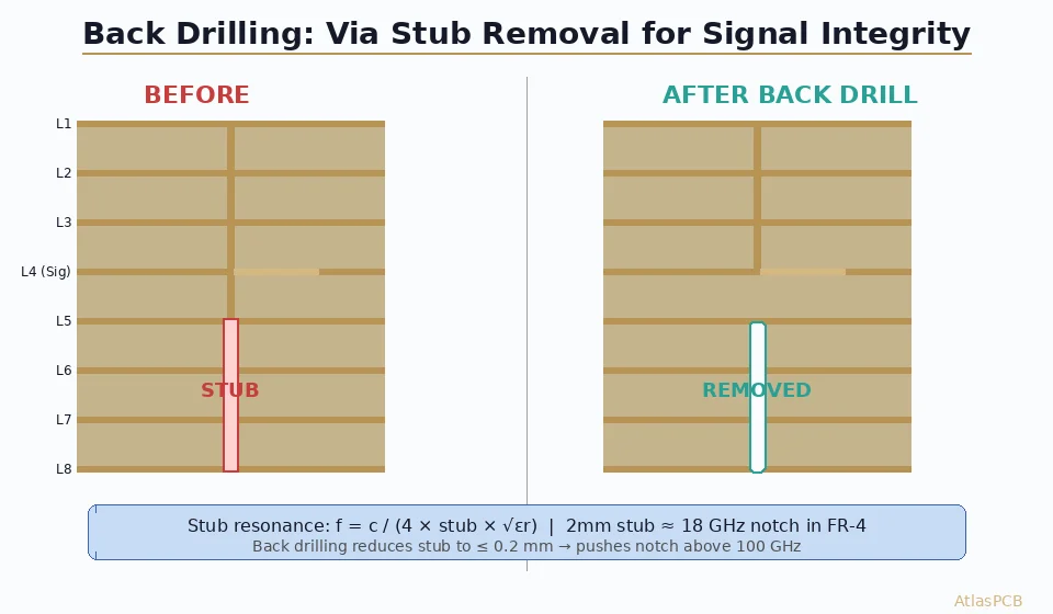
A through-hole via in a multilayer PCB creates a conductive barrel spanning the full board thickness. When a signal transitions from a trace on Layer 1 to a trace on Layer 4 of a 20-layer board, the remaining barrel from Layer 4 to Layer 20 is an unused stub. This stub behaves as a transmission line terminated in an open circuit.
The open-circuit stub produces a quarter-wave resonance at:
f_resonance = c / (4 × L_stub × √εr)
Where:
- c = speed of light (3 × 10⁸ m/s)
- L_stub = physical stub length
- εr = effective dielectric constant of the surrounding material
For a typical FR-4 stackup (εr ≈ 4.0), a 200-mil (5.08 mm) stub resonates at approximately 7.4 GHz. A 100-mil stub resonates near 14.8 GHz. At resonance, the stub presents a virtual short circuit to the signal path, causing a deep notch in the insertion loss (S21) response.
Impact on Channel Performance
| Stub Length (mil) | Stub Length (mm) | Resonant Frequency (GHz) | Effect on 10G Ethernet | Effect on 25G Ethernet |
|---|---|---|---|---|
| 300 | 7.62 | 4.9 | Severe degradation | Unusable |
| 200 | 5.08 | 7.4 | Marginal | Severe degradation |
| 100 | 2.54 | 14.8 | Minimal impact | Moderate degradation |
| 50 | 1.27 | 29.5 | Negligible | Minimal impact |
| 10 | 0.25 | >50 | Negligible | Negligible |
Beyond the primary resonance, stubs also increase broadband insertion loss through radiation and excitation of parasitic parallel-plate waveguide modes between power/ground planes. Every unnecessary mil of stub adds measurable loss above 5 GHz.
For comprehensive guidance on via geometry and its impact on signal performance, see our [signal integrity design guide]/blog/signal-integrity-pcb-design-guide/).
Back-Drilling: Stub Removal for High-Speed Channels
What Is Back-Drilling?
Back-drilling (also called controlled-depth back-drilling or counter-boring) is a post-lamination process where an oversized drill bit enters from the opposite side of the signal entry layer and removes the unused portion of the via barrel. The result is a via with a dramatically shortened stub, typically reduced to 50–200 µm (2–8 mil) of residual stub.
The Back-Drilling Process Step by Step
- Through-hole drilling: The via is drilled as a standard plated through-hole (PTH) during normal fabrication.
- Plating: The via barrel receives electroless and electrolytic copper plating.
- Outer layer imaging and etching: Pad and trace patterns are defined.
- Back-drill programming: The CNC drill program calculates the target depth based on the stackup, the signal transition layer, and the desired residual stub length.
- Back-drilling: An oversized drill bit (typically 0.2–0.3 mm larger than the original via drill) enters from the back side and removes the plated barrel to the programmed depth.
- Cleaning: Debris and drill chips are removed via high-pressure water wash and/or plasma desmear.
Back-Drill Specifications and Tolerances
| Parameter | Typical Value | Advanced Capability |
|---|---|---|
| Back-drill diameter | Original drill + 0.2 mm (8 mil) | Original drill + 0.15 mm (6 mil) |
| Depth tolerance | ±50 µm (±2 mil) | ±25 µm (±1 mil) |
| Residual stub target | 150 µm (6 mil) | 50 µm (2 mil) |
| Maximum aspect ratio (depth:diameter) | 8:1 | 12:1 |
| Minimum remaining dielectric | 100 µm (4 mil) | 75 µm (3 mil) |
| Drill bit life (hits) | 500–1,000 | Monitored per-hit with wear compensation |
| Registration accuracy | ±50 µm (±2 mil) | ±25 µm (±1 mil) |
Design Considerations for Back-Drilling
Pad sizing: The back-drill pad on the entry side must be large enough to accommodate the oversized drill plus registration tolerances. A typical rule: back-drill pad diameter = back-drill bit diameter + 2 × registration tolerance + 0.15 mm margin. For a 0.5 mm back-drill bit with ±50 µm registration, the minimum pad is 0.5 + 0.10 + 0.15 = 0.75 mm.
Anti-pad clearance: Internal layers that the back-drill passes through must have anti-pads sized for the larger back-drill diameter, not the original PTH diameter. Missing this is the most common back-drill design error.
Stackup symmetry: Back-drilling from one side shifts the mechanical center of the via. For boards back-drilled from both sides (top and bottom entry signals), ensure the stackup supports both depths without the drills colliding in the middle.
Net connectivity verification: After back-drilling, any internal layer connections originally made through the removed barrel section are severed. Your design tool’s net connectivity check must account for back-drill depth.
For a deeper dive into back-drill technology and its applications, read our guide on [PCB back drill technology]/blog/pcb-back-drill/).
Blind Via Formation by Controlled-Depth Drilling
Mechanical Blind Vias vs. Laser Blind Vias
Blind vias connect an outer layer to one or more inner layers without penetrating the entire board. Two primary formation methods exist:
- Laser drilling: UV or CO₂ lasers ablate individual dielectric layers. Best suited for microvias with diameters ≤150 µm (6 mil) and depths of 1–2 layers. This is the standard method in [HDI PCB technology]/blog/hdi-pcb-technology/).
- Mechanical controlled-depth drilling: A CNC drill penetrates to a programmed depth. Suitable for larger via diameters (≥200 µm / 8 mil) and deeper blind vias spanning 2–6 layers.
When to Use Mechanical Blind Vias
Mechanical controlled-depth blind vias are preferred when:
- Via diameter exceeds 150 µm, making laser drilling less efficient
- The blind via must span 3 or more layers (beyond single-layer microvia depth)
- Cost constraints preclude sequential lamination (which is required for stacked or staggered microvias)
- The design requires blind vias with aspect ratios up to 1:1 (depth:diameter)
| Blind Via Type | Diameter Range | Depth Range | Aspect Ratio Limit | Formation Method |
|---|---|---|---|---|
| Laser microvia | 50–150 µm | 1 layer (50–100 µm) | 0.75:1 | UV/CO₂ laser |
| Mechanical blind via | 200–600 µm | 2–6 layers (0.2–1.5 mm) | 1:1 standard, 1.5:1 advanced | CNC depth-controlled drill |
| Through-hole via | 200–600 µm | Full board | 10:1 standard, 15:1 advanced | CNC through-drill |
For comparisons between blind, buried, and through-hole vias, see our complete [blind via vs buried via]/blog/blind-via-vs-buried-via/) guide and [PCB via types guide]/blog/pcb-via-types-guide/).
Plating Challenges in Mechanical Blind Vias
Blind vias drilled mechanically face unique plating challenges:
- Solution exchange: Electrolyte must reach the bottom of a closed-end hole. Agitation, vacuum cycling, and pulse plating improve solution penetration.
- Throwing power: The plating must deposit evenly from the rim to the bottom. Standard acid copper baths achieve 60–70% throwing power; specialized blind-via chemistries reach 80–90%.
- Void prevention: Air trapped in the blind hole during plating causes voids. Vacuum pre-treatment and horizontal plating lines mitigate this.
- Dimple specification: After plating, the via surface may show a dimple (concavity). IPC-6012 Class 3 allows a maximum dimple of 150 µm. For BGA applications requiring via-in-pad, the dimple is filled with conductive or non-conductive paste and planarized.
Depth Control for Blind Via Drilling
The drill must stop in the target copper layer or within the dielectric immediately above it. Stopping too shallow leaves an incomplete via; stopping too deep damages the layer below.
Depth referencing methods:
- Surface contact: The pressure foot or depth ring contacts the board surface, establishing z=0. Depth is measured from this reference.
- Spindle-mounted laser: A laser sensor measures the board surface position before each hit, compensating for panel warpage and thickness variation.
- Back-side contact: For thicker boards, a reference point on the opposite side provides additional accuracy.
Dielectric thickness variation is the primary enemy of blind via depth accuracy. A nominal 100 µm prepreg layer may vary ±15 µm across a panel. This variation directly adds to the depth uncertainty. Specifying prepreg with tighter thickness tolerances (±10 µm or better) improves blind via yield.
Depth-Controlled Routing and Cavity Milling
Applications of Depth-Controlled Milling
Beyond drilling round holes, controlled-depth technology extends to routing (milling) operations:
- Component cavities: Recesses for embedding components (chips, passives) within the PCB stackup to reduce overall assembly height.
- RF shielding pockets: Cavities for placing shield cans or absorber material at specific depths.
- Flex-rigid transitions: Milling away rigid layers in flex-rigid PCBs to expose the flexible core in transition zones.
- Connector recesses: Pockets for press-fit connectors or card-edge contacts that require precise depth engagement.
- Thermal management: Channels or pockets for heat spreaders or thermal interface materials positioned close to heat-generating components.
Depth-Controlled Routing Process
Depth-controlled routing uses a milling bit (end mill or router bit) instead of a drill bit. The CNC machine moves in X-Y while maintaining a programmed Z depth. Key parameters:
| Parameter | Typical Value | Notes |
|---|---|---|
| Router bit diameter | 0.8–3.0 mm | Smaller bits for fine features, larger for bulk removal |
| Depth tolerance | ±50 µm (±2 mil) | Per IPC-6012E |
| Feed rate | 0.5–2.0 m/min | Slower for tighter tolerance |
| Spindle speed | 40,000–80,000 RPM | Material-dependent |
| Surface roughness (Ra) | 3–6 µm | After routing, before cleaning |
| Minimum corner radius | 50% of bit diameter | Internal corners limited by bit geometry |
Cavity PCB Design Rules
Step cavities: Multi-depth cavities with stepped shelves require separate routing passes at different depths. Each depth level adds a tolerance stack: ±50 µm per level, so a 3-step cavity accumulates ±150 µm worst-case depth uncertainty at the deepest level.
Thin remaining dielectric: When milling close to an internal copper layer, maintain a minimum 100 µm (4 mil) dielectric buffer to prevent short circuits and ensure mechanical integrity. For flex-rigid transitions, this buffer may be reduced to 50 µm with specialized equipment.
Panel utilization: Cavity routing reduces the board’s structural integrity during processing. Large or deep cavities may require sacrificial support tabs or modified handling fixtures.
Equipment and Process Control
CNC Drill Machine Capabilities
Modern controlled-depth drilling uses high-precision CNC machines with the following capabilities:
- Z-axis resolution: 1 µm or better (servo-driven spindle)
- Depth sensing: Contact-based pressure foot (standard), laser displacement sensor (advanced), or capacitive sensing (specialized)
- Hit-count monitoring: Drill bit wear tracking per hit, with automatic tool change triggers
- Compensation algorithms: Real-time adjustment for panel warpage, thickness variation, and thermal expansion
- Multi-step drilling: Programmed peck cycles for deep holes to clear chips and prevent heat buildup
Process Control and Inspection
Pre-drill verification:
- Panel thickness mapping (multiple points) using CMM or ultrasonic gauge
- Stackup verification via cross-section coupon from the same panel set
- Drill bit diameter and length verification
In-process monitoring:
- Spindle load monitoring (detects dull bits, material anomalies)
- Depth encoder feedback per hit
- Statistical process control (SPC) on depth measurements
Post-drill inspection:
- Cross-section analysis of coupon vias (destructive, per lot)
- X-ray inspection for stub length measurement (non-destructive)
- Back-light inspection for blind via bottom integrity
- Electrical testing (continuity/isolation) per IPC-9252
IPC Standards for Controlled-Depth Drilling
| Standard | Coverage |
|---|---|
| IPC-6012E | Qualification and Performance Specification for Rigid PCBs — defines depth tolerances for back-drill and blind vias |
| IPC-2221B | Generic Standard on Printed Board Design — design guidelines for blind and buried vias |
| IPC-2226 | Sectional Design Standard for HDI Printed Boards — microvia and blind via design rules |
| IPC-6018 | Microwave End Product Board Inspection and Test — depth-controlled features in RF boards |
| IPC-9252 | Requirements for Electrical Testing of Unpopulated Printed Boards — test coverage for controlled-depth features |
Design Guidelines for Controlled-Depth Drilling
Stackup Planning
The stackup is the foundation of controlled-depth drilling success. Key principles:
- Use consistent prepreg thickness: Specify prepreg with ±10 µm or better thickness tolerance. Avoid mixing prepreg types in critical layers.
- Place signal transition layers on core layers: Cores have tighter thickness tolerance (±15 µm) than prepreg (±20–25 µm). Transitioning signals on core copper layers provides a more predictable drill target.
- Provide adequate clearance layers: Ensure at least 100 µm of dielectric between the drill target depth and adjacent copper features that must not be damaged.
- Document the stackup completely: Include nominal and tolerance values for every layer. The fabricator needs this to calculate drill depths.
Specifying Back-Drill in Fabrication Drawings
Your fabrication drawing should include:
- Back-drill symbol in the drill chart (distinct from standard PTH symbols)
- Back-drill diameter for each back-drill type
- Target layer: The deepest layer to retain connectivity (e.g., “Back-drill from Bottom to Layer 4, retain Layer 3 connection”)
- Maximum residual stub: Specify in mils or µm (e.g., “Maximum 8 mil residual stub”)
- Acceptance criteria: Reference IPC-6012E Class 2 or Class 3 as applicable
Via Design Rules for Aspect Ratio
Controlled-depth features are constrained by the aspect ratio of depth to diameter. Exceeding the limit causes drill wander, poor plating, and unreliable connections. For detailed guidance on aspect ratio constraints, see our [PCB aspect ratio via design]/blog/pcb-aspect-ratio-via-design/) guide.
| Feature Type | Maximum Aspect Ratio (Standard) | Maximum Aspect Ratio (Advanced) |
|---|---|---|
| Back-drill depth : back-drill diameter | 8:1 | 12:1 |
| Mechanical blind via depth : diameter | 1:1 | 1.5:1 |
| Through-hole via depth : diameter | 10:1 | 15:1 |
| Depth-routed cavity depth : bit diameter | 3:1 | 5:1 |
Common Failure Modes and Troubleshooting
Back-Drill Failures
| Failure Mode | Root Cause | Prevention |
|---|---|---|
| Excessive residual stub | Drill depth too shallow; panel thicker than nominal | Pre-measure panel thickness; use laser depth sensing |
| Severed target connection | Drill depth too deep; panel thinner than nominal | Add dielectric buffer; tighten prepreg tolerance |
| Drill breakage | Aspect ratio exceeded; worn bit; excessive feed rate | Enforce aspect ratio limits; monitor hit counts |
| Misregistration | Panel shift during setup; tooling hole inaccuracy | Use X-ray registration; verify tooling alignment |
| Copper burrs in back-drill hole | Dull bit; incorrect spindle speed | Control hit counts; optimize speed/feed parameters |
Blind Via Failures
| Failure Mode | Root Cause | Prevention |
|---|---|---|
| Incomplete bottom connection | Drill didn’t reach target copper | Verify prepreg thickness; increase depth margin |
| Barrel crack | Thermal stress on thin barrel wall | Optimize plating thickness; control reflow profile |
| Void in plated fill | Air entrapment during plating | Use vacuum pre-treatment; optimize plating chemistry |
| Dimple exceeds spec | Insufficient fill material or poor planarization | Adjust fill paste volume; verify planarization process |
Cost and Lead Time Considerations
Controlled-depth drilling adds cost and lead time compared to standard through-hole drilling. Understanding the drivers helps optimize your design:
Cost adders:
- Back-drilling: 5–15% adder over standard PTH, depending on hole count and number of unique depths
- Mechanical blind vias: 10–25% adder, primarily from depth programming and inspection
- Depth-controlled routing: 15–30% adder for cavity formation, driven by routing time and inspection requirements
- Cross-section verification: $200–500 per coupon set (typically 2–4 coupons per lot)
Lead time impact:
- Back-drilling: +1 day (additional drilling setup and inspection)
- Blind vias with fill and planarize: +2–3 days (plating, fill, planarization, and re-inspection)
- Cavity routing: +1–2 days (programming, routing, and inspection)
Design choices that reduce cost:
- Minimize the number of unique back-drill depths (consolidate where possible)
- Use standard back-drill diameters (0.4, 0.5, 0.6 mm) rather than custom sizes
- Specify back-drill only where signal integrity simulations confirm necessity
- Group blind vias by depth to minimize tool changes
Real-World Application: 25 Gbps Backplane Design
Consider a 24-layer, 3.5 mm thick backplane carrying 25 Gbps NRZ signals. The signal enters on Layer 1 and transitions to an inner stripline on Layer 3. Without back-drilling, the stub from Layer 3 to Layer 24 is approximately 3.0 mm (118 mil), producing a first resonance at 2.5 GHz—well below the 12.5 GHz Nyquist frequency for 25 Gbps.
Back-drill specification:
- Back-drill from Layer 24 side to Layer 4
- Back-drill diameter: 0.45 mm (18 mil) for 0.25 mm (10 mil) original via
- Target residual stub: ≤150 µm (6 mil)
- Residual stub resonance: 50+ GHz (negligible impact at 25 Gbps)
Simulated channel improvement:
| Metric | Without Back-Drill | With Back-Drill (6 mil stub) |
|---|---|---|
| Insertion loss at 12.5 GHz | -28 dB | -14 dB |
| Return loss at 12.5 GHz | -6 dB | -18 dB |
| Eye height (25 Gbps NRZ) | Closed | 45 mV |
| Channel operating margin (COM) | < 0 dB | 3.2 dB |
The difference between a closed eye and a compliant channel is entirely attributable to stub removal via back-drilling.
Getting Started with Controlled-Depth Drilling at Atlas PCB
Atlas PCB operates high-precision CNC drilling platforms with ±25 µm depth accuracy, laser-based surface referencing, and full SPC monitoring. Our engineering team reviews every controlled-depth drilling design for manufacturability before production, catching anti-pad errors, aspect ratio violations, and stackup conflicts before they reach the drill floor.
Whether you need back-drilling for a 56G PAM4 switch fabric, mechanical blind vias for a compact medical device, or depth-controlled cavities for an embedded component module, our process engineering team is ready to support your design from concept through production.
Ready to move forward? Upload your Gerbers for a free engineering review — our engineers will verify your controlled-depth drilling specifications and provide detailed DFM feedback within 24 hours.
Further Reading
- [Rogers PCB Fabrication: Material Sourcing, Lead Times & Quality Control]/blog/rogers-pcb-fabrication/)
- [PCB Manufacturer with Engineering Review: Why Human DFM Audit Matters]/blog/pcb-manufacturer-engineering-review/)
- [ENEPIG vs ENIG: Which PCB Surface Finish for Your Design?]/blog/enepig-vs-enig/)
- [PCB Surface Finish Selection — ENIG vs HASL vs OSP vs Hard Gold vs ENEPIG]/blog/pcb-surface-finish-enig-hasl-osp-hard-gold-enepig/)
- [BGA Pad Design and Via-in-Pad: How to Prevent Solder Voiding in High Pin-Count BGA Assemblies]/blog/bga-pad-design-via-in-pad-solder-voiding-prevention/)
- HDI PCB Manufacturing
About AtlasPCB — We specialize in complex PCB manufacturing for HDI, RF, and high-reliability applications. Explore our impedance-controlled PCB manufacturing . Every order includes free engineering review. Get your quote.
Reviewed by AtlasPCB Engineering Team — IPC-certified manufacturing specialists with 15+ years of production experience in HDI, RF, and high-reliability PCB fabrication. Content based on factory floor data and real customer design reviews.
- controlled-depth-drilling
- back-drilling
- blind-via
- stub-removal
- high-speed