· AtlasPCB Engineering · Engineering · 7 min read
Siemens Xpedition Standard: AI-Driven PCB Design Automation Comes to SMB Teams
Siemens' new Xpedition Standard and PADS Pro Essentials bring enterprise-grade AI PCB design automation to small and mid-sized teams — a shift that democratizes intelligent routing, design reuse, and DFM-connected workflows.
The Productivity Gap in PCB Design
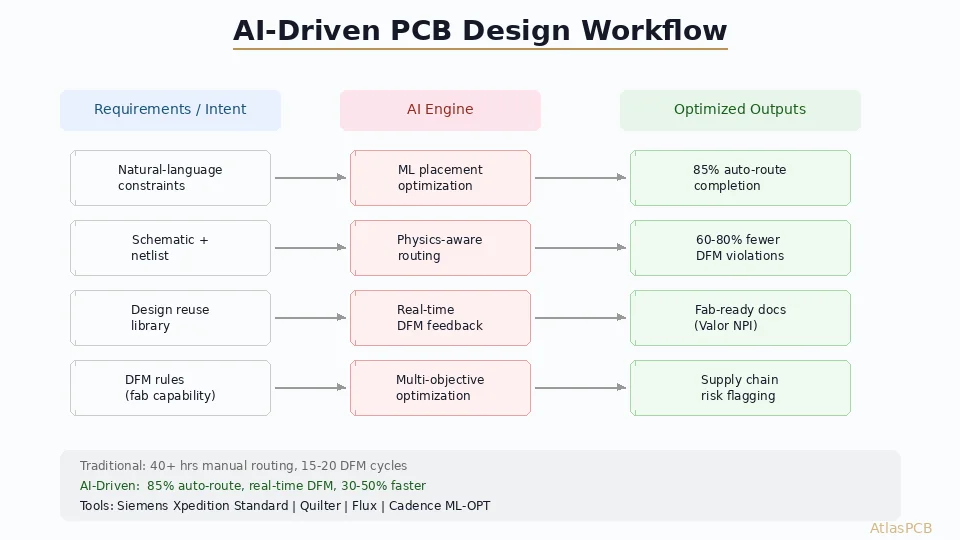
A paradox defines modern PCB engineering: tools have never been more capable, yet designers spend most of their time on repetitive execution rather than creative problem-solving. The average 8-layer board requires:
- 40+ hours of manual routing
- 15–20 DFM iteration cycles
- 8–12 hours of documentation and output generation
- Countless constraint checks and verification passes
Enterprise teams at major OEMs have long had access to AI-enhanced EDA tools that compress these timelines. But small and mid-sized electronics companies — which produce the majority of the world’s PCB designs — were locked out by $50,000+ annual licensing costs.
Siemens’ launch of Xpedition Standard and PADS Pro Essentials in 2026 changes this equation fundamentally.
What Changed: AI EDA for the Rest of Us
The Announcement
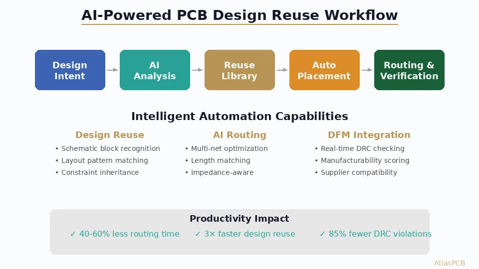
On May 18, 2026, Siemens Digital Industries Software published details of how Xpedition Standard combines four previously enterprise-only capabilities into a unified, accessible platform:
- AI-powered front-end design entry — natural-language component queries, intelligent schematic assistance
- Advanced automation for implementation — ML-driven placement optimization and routing
- Reuse-driven productivity — automated detection of reusable circuit blocks from design history
- Connected release documentation — Valor manufacturing intelligence for DFM-validated outputs
The platform specifically targets “the productivity paradox” — where increasing tool complexity has increased user burden rather than reducing it.
The Technical Architecture
Xpedition Standard is built on the same engine as enterprise Xpedition but with a curated feature set and simplified licensing:
Design Entry:
- AI-assisted schematic capture with component recommendation
- Constraint definition through natural-language intent (“route all DDR4 signals with ±5 mil length matching”)
- Automated symbol generation from manufacturer datasheets
Layout Automation:
- Physics-informed component placement optimization
- Intelligent interactive routing (ML-trained on millions of design patterns)
- Automated design rule generation from intent specifications
- Real-time DFM feedback as traces are drawn
Design Reuse:
- Automatic identification of repeated circuit blocks
- Parameterized reuse (same topology, different component values)
- Variant management across product families
- Cross-project design library with AI-tagged categorization
Manufacturing Integration:
- Valor NPI (New Product Introduction) checks during design
- Automated panelization and drill optimization
- Direct output to fabricators without manual Gerber editing
- Supply chain risk indicators integrated into BOM
How AI Routing Differs from Traditional Auto-Routing
The distinction matters because traditional auto-routing has earned justified skepticism from experienced designers. Here’s why AI-driven routing is fundamentally different:
Traditional Auto-Router (1990s–2010s)
- Rule-based: follows Manhattan or 45° algorithms
- Sequential: routes one net at a time, greedy optimization
- Context-blind: doesn’t consider SI/PI implications
- Brittle: often produces unroutable results that require manual intervention
- Static rules: same approach regardless of design context
AI-Enhanced Routing (2024+)
- Pattern-learned: trained on millions of successfully manufactured designs
- Holistic: considers all nets simultaneously with global optimization
- Context-aware: understands signal groups, differential pairs, timing constraints
- Adaptive: adjusts strategy based on board density and constraint complexity
- Iterative: runs multiple optimization passes with design-space exploration
Practical example: Routing a DDR4 byte lane requires length-matching within ±5 mils, impedance control, crosstalk avoidance between byte lanes, and via minimization. A traditional auto-router treats these as separate constraint checks applied sequentially. An AI router understands the DDR4 topology pattern and routes the entire byte lane as a coordinated group, choosing via positions and layer assignments that simultaneously satisfy all constraints.
Results in Practice
Based on published case studies from early Xpedition Standard deployments:
- 4-layer IoT boards: 85% auto-route completion (vs 40–60% with traditional tools)
- 8-layer mixed-signal: 70% auto-route completion with SI-aware routing
- 12-layer FPGA boards: 55% auto-route completion, with remaining manual routing guided by AI suggestions
- DFM violations: Reduced 60–80% through real-time feedback during routing
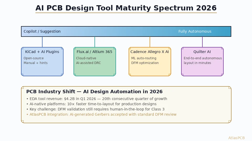
The Broader AI EDA Landscape in 2026
Siemens isn’t alone in this space. The AI PCB design ecosystem has expanded rapidly:
Quilter
- Fully autonomous PCB layout from netlist to Gerber
- Physics-driven rather than ML-trained approach
- Best for standardized designs (IoT, power supplies, simple digital)
- Published results: 10× faster than manual for compatible designs
Flux
- Raised $37M (Series B led by 8VC) for AI-first PCB design
- Cloud-native, collaborative design environment
- Strong integration with component databases and simulation
- Targeting the “Google Docs of PCB design” model
Cadence ML-OPT
- Machine learning for constraint optimization in Allegro
- Focuses on signal integrity and power integrity automation
- Enterprise-tier pricing, targeting advanced designs (20+ layers)
What Makes Xpedition Standard Different
Siemens’ advantage is the manufacturing connection. While Quilter and Flux optimize the design phase, Xpedition Standard integrates Valor manufacturing intelligence throughout:
- DFM rules are checked as you route (not post-design)
- Panelization is optimized automatically
- Fabricator capability constraints are built into routing decisions
- BOM supply chain risks are visible during component selection
This closed loop between design and manufacturing is where the real productivity gain lies — eliminating the 3–5 DFM revision cycles that typically add 2–4 weeks to a project.
ATLAS PCB — DESIGN-TO-MANUFACTURING PARTNER
AI-Designed Boards Still Need Expert Manufacturing
Whether your layout comes from Xpedition, Altium, KiCad, or an AI tool — our engineering team validates DFM, optimizes panelization, and ensures your design manufactures perfectly on the first run.
Upload Design for DFM Review →Impact on PCB Manufacturing
AI design automation doesn’t just affect designers — it ripples through the entire supply chain:
Better DFM Compliance = Higher First-Pass Yield
When AI tools enforce manufacturing constraints during design (not after), fabricators receive designs that are inherently manufacturable. This means:
- Fewer engineering questions (ECQ) during quoting
- Higher panel yield (fewer DFM-violation-induced defects)
- Faster time-to-first-article
- Reduced NRE iterations
Faster Design Cycles = More Prototyping Volume
If AI compresses a 4-week design cycle to 2 weeks, hardware teams iterate twice as fast. This increases prototype PCB volume — good news for quick-turn fabricators.
Standardized Outputs = Streamlined Quoting
AI tools generate clean, complete fabrication packages. No more missing drill files, incorrect stackup notes, or ambiguous impedance specs. This reduces quoting time from hours to minutes for standard boards.
The Manufacturing Knowledge Gap Remains
However, AI design tools don’t eliminate the need for manufacturing expertise:
- Material selection still requires understanding of supply chain availability
- Advanced processes (sequential lamination, laser drilling, back-drilling) need human engineering judgment
- Yield optimization for high-volume production requires fab-specific tuning
- Quality requirements (IPC class, automotive qualification) must be correctly specified
What This Means for Hardware Teams
Small Teams (1–5 Engineers)
The biggest beneficiaries. A 2-person hardware startup can now achieve design productivity comparable to a 10-person team using traditional tools:
- AI handles the routing grind
- Design reuse accelerates derivative products
- Built-in DFM eliminates costly redesign cycles
- Cloud collaboration enables distributed teams
Mid-Sized Companies (5–50 Engineers)
Standardization benefits compound: design libraries grow through AI-tagged reuse, institutional knowledge persists through tool-captured best practices, and junior engineers become productive faster with AI guidance.
Large Enterprises
Already have access to full Xpedition. But the democratization of AI design tools means their supply chain partners and contract design houses now deliver higher-quality designs — reducing incoming DFM issues.
The Future: AI Across the Hardware Development Loop
The current wave of AI EDA tools optimizes design execution — the routing, placement, and verification steps. The next evolution will address:
- Architecture exploration — AI suggesting optimal component selection and block diagrams based on specifications
- Multi-physics co-optimization — simultaneously optimizing thermal, SI, PI, and EMC
- Manufacturing-aware synthesis — designs generated with specific fabricator capabilities as constraints
- Predictive reliability — AI estimating MTBF based on design choices and environmental conditions
- Autonomous NPI — from specification to manufactured prototype with minimal human intervention
Implications for PCB Fabricators
As AI-designed boards become the norm, fabricators should prepare:
- Accept AI-generated fabrication packages — these will be more standardized but may use less conventional output formats
- Provide machine-readable capability files — AI tools need structured data about your process capabilities (minimum trace width, via aspect ratio, impedance tolerance, etc.)
- Invest in automated DFM engines — incoming designs will be “mostly DFM-clean” but still need validation against specific factory capabilities
- Differentiate on advanced capabilities — when basic DFM is handled by AI, fabricators compete on exotic processes, tight tolerances, and reliability testing
Further Reading
- [AI-Powered EDA Tools in 2026: How Autonomous Agents Reshape PCB Design]/blog/ai-powered-eda-pcb-design-autonomous-agents-2026/)
- [PCB Laser Direct Imaging (LDI): Resolution Advantages Over Phototool Lithography]/blog/pcb-laser-direct-imaging-ldi-vs-phototool/)
- [Controlled Impedance PCB Design: Stackup Calculations and Manufacturing]/blog/controlled-impedance-pcb-design-stackup-calculations/)
- [HDI PCB Stackup Design: Advanced Techniques]/blog/hdi-pcb-stackup-design-advanced/)
Using AI tools to design your next PCB? AtlasPCB works with outputs from any EDA platform — including AI-generated designs from Quilter, Flux, and Xpedition Standard. Get a quote for your AI-designed board →
About AtlasPCB — We specialize in complex PCB manufacturing for HDI, RF, and high-reliability applications. Explore our full PCB manufacturing capabilities, or get an instant online quote . Every order includes free engineering review. Get your quote.
Reviewed by AtlasPCB Engineering Team — IPC-certified manufacturing specialists with 15+ years of production experience in HDI, RF, and high-reliability PCB fabrication. Content based on factory floor data and real customer design reviews.
- ai pcb design
- eda tools
- siemens xpedition
- design automation
- pcb routing
- design reuse
- pads pro
- smb electronics