· AtlasPCB Engineering · Engineering · 9 min read
DC-DC Converter PCB Layout: Hot Loop Optimization and EMI Reduction Techniques
Learn critical PCB layout techniques for DC-DC buck and boost converters. Covers hot loop minimization, component placement, ground plane strategies, and thermal management for switching regulators from 100kHz to 5MHz.
The Foundation: Understanding Switching Converter Current Paths
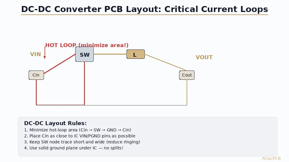
Every switching DC-DC converter has two fundamental current loops that alternate at the switching frequency. Understanding these loops is the absolute prerequisite for good layout:
Loop 1 — High-side ON (buck converter): Input supply → Input capacitor → High-side FET (or internal switch) → Inductor → Output capacitor → Load → Return through ground plane → Back to input capacitor.
Loop 2 — Low-side ON (buck converter): Inductor → Output capacitor → Load → Return through ground → Low-side FET (or synchronous rectifier) → Back to inductor.
The critical distinction: Loop 1 carries the high-frequency switching transient (the “hot loop”) because current transitions between zero and full load current in nanoseconds during switching edges. Loop 2 carries relatively smooth inductor current with low di/dt.
Hot Loop: The #1 Layout Priority
The hot loop area directly determines radiated EMI per the relationship:
E_radiated ∝ f² × A × I_peakWhere f is switching frequency, A is loop area, and I_peak is peak switching current. At modern switching frequencies (1-5 MHz), even 5mm² of extra loop area creates measurable EMI increases.
Identifying the Hot Loop
For a synchronous buck converter IC (integrated high-side and low-side FETs):
Hot Loop Path:
CIN(+) → VIN pin → [internal high-side FET] → SW pin →
[external inductor] → [this part is NOT hot loop!]
...actually the hot loop is:
CIN(+) → VIN pin → [internal switches] → PGND pin → CIN(-)
The key insight: the inductor is NOT in the hot loop. The inductor acts as a current source—its current changes slowly (limited by L×di/dt = V). The hot loop is the input capacitor to VIN to PGND loop, where current switches from zero to peak in 2-10 nanoseconds.
Minimization Strategies
Strategy 1: Place CIN adjacent to IC (mandatory)
The input ceramic capacitor (4.7μF-22μF X7R) must be the closest component to the VIN and PGND pins. Target:
- Distance VIN pin to CIN pad: <2mm
- Distance PGND pin to CIN pad: <2mm
- Both connections on the same layer (avoid vias in the hot loop path)
Strategy 2: Orient CIN to minimize loop
Rotate the capacitor so its terminals face the VIN and PGND pins directly. A 0402 or 0603 CIN oriented parallel to the IC pin row creates shorter traces than perpendicular placement.
Strategy 3: Use both sides of the PCB
For IC packages with exposed thermal pads (most modern converters), place CIN on the bottom layer directly beneath the IC. Connect through multiple vias (4-6 minimum) to reduce via inductance. This creates the absolute minimum loop area—current flows vertically through the board thickness (1.6mm or less) rather than laterally.
Strategy 4: Multiple CIN capacitors
For high-current converters (>5A), use 2-3 input capacitors in parallel, placed as close as possible to the IC. This reduces effective ESR and ESL while sharing the ripple current. Arrange them symmetrically around the VIN/PGND pins.
Complex Power Supply PCB Design?
AtlasPCB fabricates multi-layer power boards with heavy copper, embedded coin, and tight impedance control for demanding DC-DC converter applications.
Request a Power PCB Quote →Switch Node: The Noisiest Net
The switch node (SW) experiences the fastest voltage transitions on the board—slew rates of 10-50 V/ns are common. This makes the SW node copper area a primary radiator.
Layout Rules for Switch Node
Keep it short but not tiny: The trace from the IC SW pin to the inductor should be as short as possible (ideally <5mm) to minimize antenna length, but wide enough to carry DC current without excessive heating.
Minimize copper area: Unlike power and ground planes where bigger is better, the SW node copper should be the minimum size needed for current capacity and thermal dissipation. Excessive SW node copper acts as a radiating antenna.
No vias if possible: Route the SW node on a single layer from IC to inductor. Each via adds 0.5-1 nH of inductance and creates a potential radiation point.
Shield with ground: Place ground copper on adjacent layers above and below the SW node trace. This capacitively couples the high-frequency noise to ground rather than letting it radiate.
Boot capacitor placement: The bootstrap capacitor (CBOOT) must be close to the BOOT and SW pins. The boot loop should be minimized with the same rigor as the input hot loop.
Ground Plane Design
Solid Ground Plane: Non-Negotiable
The ground plane directly beneath the converter IC must be solid and unbroken. This provides:
- Lowest impedance return path for switching currents
- EMI shielding for layers below
- Thermal heat spreading from the IC thermal pad
- Impedance reference for any controlled impedance routing nearby
Ground Connections from Thermal Pad
Most modern DC-DC ICs use an exposed pad for ground connection and thermal dissipation. Connect it to the ground plane with:
- Minimum 9 vias (3×3 array) for adequate thermal and electrical connection
- Via drill: 0.3mm, finished hole 0.2mm
- Via spacing: 1.0-1.2mm center-to-center
- Fill vias with epoxy if assembling with reflow to prevent solder wicking
Kelvin Sense Connections
For ICs with separate PGND (power ground) and SGND (signal ground) pins:
- Connect both to the same ground plane
- Route SGND as a separate trace from the IC pin to the ground plane, not through the high-current PGND path
- The PGND carries switching current; SGND carries only milliamp-level reference currents
- A shared via or copper pour that carries both PGND switching noise and SGND reference signal will corrupt internal voltage references
Inductor Placement and Routing
Inductor Position
The inductor connects the noisy switching domain (SW node) to the quiet output domain. Position it to:
- Minimize SW node trace length from IC to inductor pad 1
- Allow short, wide connection from inductor pad 2 to output capacitor
- Maintain clearance from sensitive analog circuitry (feedback divider, reference)
- Provide thermal dissipation path (large copper pad around inductor footprint)
Inductor Copper Pour
Extend the output-side inductor pad into a large copper pour that connects directly to the output capacitor. This pour:
- Reduces DC resistance for output current
- Provides thermal mass for inductor cooling
- Creates low-impedance path to COUT
Magnetic Field Consideration
Shielded inductors (metal composite or toroid) contain their magnetic flux internally. Unshielded inductors radiate significant magnetic field within 5-10mm. For unshielded designs:
- Keep sensitive traces (feedback, compensation) at least 10mm from the inductor
- Orient the inductor so its field axis doesn’t couple into nearby signal traces
- Place a ground plane below the inductor on the immediate adjacent layer
Output Capacitor Placement
Output capacitors filter the inductor ripple current. Their placement is less critical than CIN because the current they carry is triangular (smooth) rather than trapezoidal (sharp edges).
Key rules:
- Place COUT within 5mm of the inductor output pad
- Connect output capacitor ground directly to the ground plane (short via, wide trace)
- For multi-capacitor arrays, arrange them closest-to-furthest from the inductor
- The feedback voltage sense point should connect at the COUT pad, not the IC output—this ensures the regulation point is at the load, not at the IC
Feedback Network Layout
The voltage feedback divider and compensation network carry microamp-level signals but directly control output voltage accuracy. Layout errors here cause noise injection and regulation degradation.
Critical Rules:
Route feedback trace away from SW node: Minimum 5mm separation, preferably on different layers with ground shielding between them.
Short traces for divider resistors: Place the feedback resistor divider close to the FB/COMP pin, not close to the output capacitor. The FB pin input impedance is extremely high—long traces act as antennas.
Ground reference: Connect the bottom feedback resistor ground directly to a quiet ground point near the IC SGND pin, not to the power ground carrying switching currents.
Compensation components: Place RC compensation components (on COMP pin) immediately adjacent to the IC. These set loop dynamics—parasitic capacitance from long traces can cause instability.
Thermal Management
IC Thermal Pad Design
The exposed thermal pad is the primary heat dissipation path. For a typical 3A buck converter dissipating 0.5W:
- Thermal pad copper area: minimum 100mm² per 0.5W (more is better)
- Via array to internal ground planes for thermal conduction
- Place on at least 2oz copper for better lateral spreading
- Calculate junction temperature: Tj = Ta + Pd × θJA
High-Current Output Path
For converters above 5A, the output copper (inductor to COUT to load connector) carries continuous DC current. Size the trace/pour for acceptable temperature rise:
- 1oz copper: ~35 mils (0.9mm) width per ampere for 10°C rise
- 2oz copper: ~17 mils (0.43mm) width per ampere for 10°C rise
- Use copper fills rather than traces for power paths
- Multiple vias in parallel for layer transitions (each 0.3mm via carries ~1A)
Thermal Via Arrays
Under high-power ICs, thermal via arrays transport heat to inner layers and the bottom copper:
- Recommended: via-in-pad with filled vias under the thermal pad
- Array density: one via per 1-1.5mm² of thermal pad area
- Connect vias to a thermal relief-free pad on internal planes for maximum heat flow
- Bottom copper: provide exposed copper or thermal pad for heatsink attachment
Common Mistakes and Their Consequences
Mistake 1: Input capacitor too far from IC
- Symptom: Excessive voltage ringing on VIN, failed EMI pre-compliance
- Fix: Relocate CIN within 2mm of VIN/PGND pins
Mistake 2: Via in the hot loop path
- Symptom: Added inductance causes higher voltage spikes, ringing
- Fix: Route CIN to IC on same layer, no vias in critical path
Mistake 3: Ground plane split under converter
- Symptom: High CM noise, ground bounce, poor regulation
- Fix: Solid ground plane; use distance for isolation instead
Mistake 4: Long SW node trace
- Symptom: Radiated EMI failure at switching frequency harmonics
- Fix: Minimize SW trace to <5mm, reduce copper area
Mistake 5: Feedback trace routed near inductor
- Symptom: Jittery output voltage, oscillation under certain loads
- Fix: Route FB trace on quiet layer, shield with ground, keep 10mm from inductor
Multi-Converter Board Layout
Modern boards often have 5-10+ DC-DC converters. Additional considerations:
- Separate input power entry: Each converter’s CIN should have a dedicated connection to the input power rail, not daisy-chained
- Converter isolation: Maintain >10mm between converter ICs; place ground fill between them
- Clock synchronization: If converters are synced to an external clock, route the SYNC signal as a controlled-impedance trace with ground reference
- Sequencing: Keep enable/PGOOD signals away from switching nodes
- Thermal zones: Don’t cluster all converters together—distribute thermal dissipation across the board
Further Reading
- PCB Power Integrity and Decoupling Design
- PCB Thermal Via Array Design Rules for Power Electronics
- GaN and SiC Power Device PCB Thermal Layout
- EMI/EMC PCB Design Fundamentals
Designing a high-current power supply PCB? Our fabrication process supports 4oz+ copper, thermal coin embedding, and controlled impedance for integrated power/signal boards. Get a manufacturing quote →
About AtlasPCB — We specialize in complex PCB manufacturing for HDI, RF, and high-reliability applications. Explore our heavy copper PCB manufacturing, aluminum and metal-core PCB services, or get an impedance-controlled PCB manufacturing . Every order includes free engineering review. Get your quote.
Reviewed by AtlasPCB Engineering Team — IPC-certified manufacturing specialists with 15+ years of production experience in HDI, RF, and high-reliability PCB fabrication. Content based on factory floor data and real customer design reviews.
- DC-DC converter
- PCB layout
- power electronics
- EMI
- hot loop
- buck converter
- switching regulator
- thermal management