· AtlasPCB Engineering · Engineering · 7 min read
OSP vs ENIG Surface Finish: Cost, Shelf Life, and Assembly Decision Guide
Direct comparison of OSP and ENIG surface finishes for PCB manufacturing. Covers cost per pad, shelf life, reflow compatibility, and when each finish makes engineering and commercial sense.
30-Second Decision: OSP or ENIG?
| Factor | OSP | ENIG |
|---|---|---|
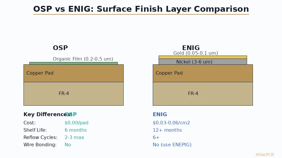
| Cost premium | Near zero | $0.03-0.06/cm2 |
| Shelf life | 6 months (sealed) | 12+ months |
| Max reflow cycles | 2-3 | 6+ |
| Pad planarity | Follows copper | Extremely flat |
| Fine-pitch BGA (<0.5mm) | Marginal | Excellent |
| ICT/probe contact | Poor | Excellent |
| Wire bonding | No | No (use ENEPIG) |
| Press-fit pins | Not recommended | Good |
| Lead-free compatible | Yes | Yes |
| Visual inspection | Difficult (transparent) | Easy (gold surface) |
Quick rule: If your board ships to assembly within 4 weeks and uses only standard SMT components, OSP saves money without technical risk. If you stock bare boards, use fine-pitch BGAs, or need multiple thermal cycles, ENIG is the engineering choice.
How Each Finish Works
OSP (Organic Solderability Preservative)
OSP deposits a water-based organic compound (typically benzimidazole or benzotriazole derivative) onto clean copper. The resulting film is 0.2-0.5 um thick — just enough to prevent copper oxidation until soldering.
During reflow, the organic film decomposes at soldering temperatures, exposing fresh copper for metallurgical bonding with solder. The process is simple:
- Micro-etch copper surface
- Apply organic compound via conveyorized spray or dip
- Rinse and dry
Total processing time: 5-8 minutes. No waste treatment for heavy metals.
ENIG (Electroless Nickel Immersion Gold)
ENIG deposits a dual-layer coating: 3-6 um of electroless nickel-phosphorus alloy, topped with 0.05-0.1 um of immersion gold. The nickel forms the actual solder joint barrier; the gold prevents nickel oxidation during storage.
The process involves:
- Micro-etch and activate copper
- Electroless nickel deposition (15-25 minutes bath)
- Immersion gold displacement (8-12 minutes)
- Rinse and dry
Total processing time: 40-60 minutes. Requires careful bath chemistry control to avoid the “black pad” defect (nickel hyper-corrosion during gold deposition).
Cost Analysis: When Does ENIG Pay for Itself?
The raw finish cost difference is straightforward:
| Board Size | OSP Cost | ENIG Cost | Delta |
|---|---|---|---|
| 50x50mm prototype (5 pcs) | ~$0 | +$3-5 | Negligible |
| 100x100mm (50 pcs) | ~$0 | +$15-30/panel | Moderate |
| 200x300mm production (1000+) | ~$0 | +$150-350/lot | Significant |
But cost analysis must include downstream failure costs:
- Rework due to oxidation: A single OSP board that arrives at assembly with copper tarnish costs $15-50 to rework or scrap
- Rejected lots: If OSP boards exceed shelf life before assembly, entire lots may require re-finishing or scrapping
- Testing probe damage: ICT fixtures contacting oxidized OSP pads wear faster and give false failures
For medium-volume production with predictable JIT assembly schedules, OSP offers genuine savings. For prototype and NPI (new product introduction) boards that may sit in inventory, ENIG eliminates logistics risk.
SURFACE FINISH SELECTION
Not Sure Which Finish Fits Your Design?
Upload your Gerber files and our engineers will recommend the optimal surface finish based on your BOM, assembly process, and lead time requirements.
Get Finish Recommendation ›Assembly Compatibility: Where OSP Falls Short
Multiple Reflow Cycles
Double-sided SMT boards require two reflow passes. OSP degrades with each thermal excursion:
- After 1st reflow: ~90% of pads remain solderable
- After 2nd reflow: ~70% solderability (increased wetting failures on fine-pitch)
- After 3rd reflow: Unacceptable for production (>5% wetting defects typical)
ENIG maintains >99% solderability through 6+ reflow cycles because the nickel-gold barrier is metallic, not organic.
Wave Soldering and Selective Soldering
Through-hole components assembled after SMT reflow expose the OSP coating to a third thermal cycle. If your assembly flow is:
- Top-side SMT reflow
- Bottom-side SMT reflow
- Wave/selective solder for connectors
Then OSP is a technical risk. The exposed through-hole pads may oxidize between steps 2 and 3, especially if work-in-process sits overnight.
Press-Fit Connectors
High-force press-fit pins (Samtec, TE Connectivity, Harting) require a hard, wear-resistant pad surface. The thin OSP film provides no mechanical protection — pins can scrape through to raw copper, and the insertion force measurement becomes unreliable. ENIG’s nickel layer acts as a hard bearing surface that maintains consistent press-fit retention force.
In-Circuit Testing (ICT)
Test probe tips (typically beryllium copper or spring-loaded) make better electrical contact with ENIG’s metallic gold surface than with OSP’s organic film. OSP boards often require higher probe forces, which accelerates fixture wear and increases false-failure rates. For high-volume production with 100% ICT, the fixture cost savings from ENIG often exceed the finish cost premium.
MULTI-STEP ASSEMBLY
Complex Assembly? Let Us Match the Finish to Your Process
Double-sided reflow, wave solder, press-fit -- we select surface finish based on your complete assembly sequence.
Upload Design Files ›When OSP Is the Right Choice
OSP excels in specific scenarios:
1. High-volume consumer electronics with JIT assembly Manufacturers like Foxconn and Pegatron use OSP on >60% of smartphone and laptop boards because:
- Boards move from fabrication to assembly within 1-2 weeks
- Assembly lines are optimized for single or double reflow only
- Cost savings at 100K+ unit volumes are substantial
2. LED lighting boards Single-sided aluminum or FR-4 LED boards with simple assembly (one reflow pass) benefit from OSP’s low cost without downside.
3. Automotive body electronics (non-safety) Interior lighting, seat control, and infotainment modules use OSP where the supply chain guarantees rapid assembly after fabrication.
4. Boards where environmental credentials matter OSP processing uses no heavy metals (no nickel, no gold) and generates no hazardous waste. Some EU OEMs specify OSP for RoHS+ compliance and sustainability reporting.
When ENIG Is the Right Choice
1. Prototype and NPI boards Unknown assembly timeline, potential redesigns, boards stored for weeks or months between design iterations.
2. Any board with BGA pitch below 0.5mm The pad planarity requirements for fine-pitch BGAs make ENIG mandatory for reliable solder paste deposition.
3. Mixed-technology assembly (SMT + through-hole + press-fit) Multiple thermal cycles and mechanical insertion demands exceed OSP capability.
4. Products requiring field rework Service technicians replacing components months or years later need solderable pad surfaces. ENIG maintains solderability indefinitely under conformal coating.
5. RF and high-frequency boards While both finishes work electrically, ENIG provides more consistent contact resistance for edge-launch SMA connectors and RF board performance at mmWave frequencies.
PROTOTYPE ORDERS
Quick-Turn Prototypes with ENIG Standard
AtlasPCB includes ENIG at no extra charge on prototype orders under 10 pcs. Maximum shelf life for your iteration cycles.
Get Instant Quote ›Decision Flowchart
Follow this logic for your next board:
Will board be assembled within 4 weeks of fabrication?
- No → ENIG
- Yes → Continue
Does assembly require more than 2 thermal cycles?
- Yes → ENIG
- No → Continue
Are there fine-pitch BGAs (<0.5mm) or press-fit connectors?
- Yes → ENIG
- No → Continue
Is ICT (in-circuit testing) required at production volume?
- Yes → ENIG (reduces probe wear and false failures)
- No → Continue
Is unit cost the primary optimization target?
- Yes → OSP
- No → ENIG (default safe choice)
For boards that genuinely need neither — consider Immersion Silver or Immersion Tin as middle-ground options with 9-month shelf life and moderate cost.
ATLASPCB
Ready to Order? All Surface Finishes Available
OSP, ENIG, ENEPIG, Immersion Silver, Immersion Tin, Hard Gold, HASL -- select at checkout or let us recommend based on your assembly process.
Compare Prices ›Related Reading:
About AtlasPCB — We specialize in complex PCB manufacturing for HDI, RF, and high-reliability applications. Explore our RF and high-frequency PCB services, PCB assembly services, or get an full PCB manufacturing capabilities . Every order includes free engineering review. Get your quote.
Reviewed by AtlasPCB Engineering Team — IPC-certified manufacturing specialists with 15+ years of production experience in HDI, RF, and high-reliability PCB fabrication. Content based on factory floor data and real customer design reviews.
- OSP
- ENIG
- surface finish
- PCB assembly
- soldering
- shelf life
- cost comparison