· AtlasPCB Engineering · Engineering · 11 min read
Fine-Pitch SMT Pad Design: 0201 to BGA
Engineering guide to fine-pitch SMT pad design for 0201, 01005, and ultra-fine BGA landing patterns.
The Challenge of Fine-Pitch SMT Assembly
The relentless push toward miniaturization drives PCB pad design into increasingly demanding territory. Metric 0201 components (imperial 008004, body size 0.25 mm × 0.125 mm) are now mainstream in smartphones and wearables. Metric 01005 (imperial 004002, body size 0.125 mm × 0.0625 mm) appears in advanced RF front-end modules. Ultra-fine-pitch BGAs at 0.3 mm and 0.25 mm pitch are standard in mobile processors and FPGA packages.
At these scales, every design decision matters. A 25 µm error in pad geometry can mean the difference between 99.9% yield and a 5% defect rate. Tombstoning, bridging, insufficient solder, and head-in-pillow defects all become more frequent as pitch decreases.
This guide provides actionable pad design recommendations for 0201, 01005, and ultra-fine BGA components, with real dimensions, stencil design rules, and DFM considerations. For broader pad design principles for BGA and QFN packages, see our [PCB pad design BGA QFN guide]/blog/pcb-pad-design-bga-qfn/).
Component Size Reference
Understanding the naming conventions is essential, as imperial and metric designations are easily confused:
| Metric Name | Imperial Name | Body L × W (mm) | Typical Use |
|---|---|---|---|
| 1005 | 0402 | 1.0 × 0.5 | General passives, IoT |
| 0603 | 0201 | 0.6 × 0.3 | Smartphones, wearables |
| 0402 | 01005 | 0.4 × 0.2 | RF modules, SiP |
| 0201 | 008004 | 0.25 × 0.125 | Advanced SiP, medical |
| 01005 | 004002 | 0.125 × 0.0625 | Research, ultra-miniature |
Note: This article uses metric designations throughout unless explicitly stated otherwise. The metric 0201 is the imperial 008004; the metric 01005 is the imperial 004002.
Pad Design for Metric 0603 (Imperial 0201)
The metric 0603 component is now the most common passive size in consumer electronics. It is well within the capability of modern assembly lines, but still requires careful pad design.
Recommended Pad Geometry
Based on IPC-7351B Level B (nominal density) and validated production data:
| Parameter | Dimension (mm) | Notes |
|---|---|---|
| Pad width (X) | 0.30 | Matches component terminal width |
| Pad length (Y) | 0.30 | Provides adequate solder fillet |
| Gap between pads | 0.20 | Prevents bridging |
| Overall footprint span | 0.80 | Center-to-center |
| Solder mask clearance | 0.05 per side | From pad edge |
| Solder paste reduction | 0% | Full aperture at 0.10 mm stencil |
Stencil Design
For 0.10 mm (4 mil) stencil thickness:
- Aperture size: 0.28 mm × 0.28 mm (slight reduction from pad for paste alignment)
- Area ratio: (0.28 × 0.28) / (2 × (0.28 + 0.28) × 0.10) = 0.70 ✓ (above 0.66 threshold)
- Shape: Rounded corners (0.03 mm radius) improve paste release
Pad Design for Metric 0402 (Imperial 01005)
Moving to metric 0402 significantly increases assembly difficulty. Component placement accuracy must be within ±0.025 mm, and solder paste volume becomes the dominant yield variable.
Recommended Pad Geometry
| Parameter | Dimension (mm) | Notes |
|---|---|---|
| Pad width (X) | 0.20 | Slightly wider than terminal |
| Pad length (Y) | 0.20 | Minimal fillet, controlled volume |
| Gap between pads | 0.15 | Tight but sufficient for 0.08 mm stencil |
| Overall footprint span | 0.55 | Center-to-center |
| Solder mask clearance | 0.04 per side | Precision registration required |
| Solder paste reduction | 10% per side | Prevents excess volume |
Stencil Design
For 0.08 mm (3 mil) stencil thickness:
- Aperture size: 0.18 mm × 0.18 mm
- Area ratio: (0.18 × 0.18) / (2 × (0.18 + 0.18) × 0.08) = 0.56 — below 0.66 threshold
- Mitigation: Use electropolished or nano-coated stencil to improve paste release
- Alternative: Reduce stencil to 0.06 mm (2.5 mil) and increase aperture to 0.19 mm × 0.19 mm:
- Area ratio: (0.19 × 0.19) / (2 × (0.19 + 0.19) × 0.06) = 0.79 ✓
Critical Assembly Requirements
- Placement accuracy: ±0.025 mm (machine capability, not just specification)
- Paste type: Type 5 (15–25 µm particle) or Type 6 (5–15 µm) solder paste
- Reflow profile: Nitrogen atmosphere (<500 ppm O₂) strongly recommended
- Board flatness: <75 µm warp over component area
- Fiducial accuracy: Local fiducials within 10 mm of 0402 cluster
Pad Design for Metric 0201 (Imperial 008004)
Metric 0201 represents the current frontier of passive component assembly. Only a handful of contract manufacturers worldwide offer reliable volume production at this scale.
Recommended Pad Geometry
| Parameter | Dimension (mm) | Notes |
|---|---|---|
| Pad width (X) | 0.12 | Near terminal edge |
| Pad length (Y) | 0.14 | Controlled extension |
| Gap between pads | 0.10 | Absolute minimum for paste separation |
| Overall footprint span | 0.36 | Center-to-center |
| Solder mask clearance | 0.03 per side | LDI solder mask required |
| Solder paste reduction | 15% per side | Volume control critical |
Stencil Design
For 0.05 mm (2 mil) stencil thickness:
- Aperture size: 0.10 mm × 0.12 mm
- Area ratio: (0.10 × 0.12) / (2 × (0.10 + 0.12) × 0.05) = 0.55
- Nano-coated, laser-cut, electropolished stencil mandatory
- Consider: Step-down stencil with local 0.04 mm thickness for 0201 area
Fabrication Requirements
At the metric 0201 scale, PCB fabrication capability becomes a gating factor:
- Minimum trace/space: 0.050 mm / 0.050 mm (2 mil / 2 mil) for routing between pads
- Solder mask: Laser direct imaging (LDI) with ±0.020 mm registration
- Copper thickness: 12 µm (1/3 oz) base copper for etch accuracy
- Surface finish: ENEPIG or immersion gold preferred (flat surface critical)
- Pad-to-pad variation: <±0.015 mm across the panel
These requirements push beyond standard fabrication capabilities. Review our [PCB design rules trace width spacing]/blog/pcb-design-rules-trace-width-spacing/) article for compatibility.
Ultra-Fine BGA Landing Pad Design
Ball Grid Array packages continue to shrink in pitch. While 0.8 mm and 0.65 mm pitch BGAs are well understood, 0.4 mm and 0.3 mm pitch designs require fundamentally different approaches.
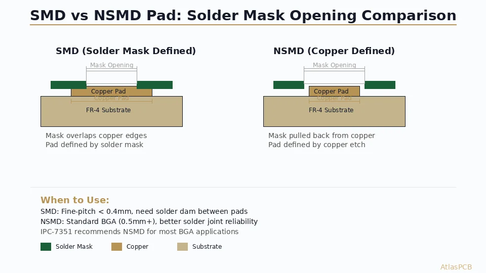
NSMD vs. SMD Pad Definition
For BGA pads, two solder mask approaches exist:
Non-Solder-Mask-Defined (NSMD): The copper pad is smaller than the solder mask opening. Pad size is controlled by copper etching (±0.025 mm).
Solder-Mask-Defined (SMD): The solder mask overlaps the copper, and the exposed copper area is defined by the mask opening. Pad size is controlled by solder mask registration (±0.050 mm).
| Parameter | NSMD | SMD |
|---|---|---|
| Pad size tolerance | ±0.025 mm | ±0.050 mm |
| Solder joint shape | Barrel-shaped (stronger) | Hourglass (weaker) |
| Preferred for pitch | ≥0.4 mm | <0.3 mm |
| Electrical test | Probe on annular ring | Probe on via (if via-in-pad) |
| Trace routing | Easier breakout | Harder breakout |
Recommendation: Use NSMD for ≥0.4 mm pitch. For 0.3 mm pitch and below, SMD or hybrid approaches (NSMD with tight solder mask registration) may be necessary because the copper pad and solder mask opening dimensions converge.
0.4 mm Pitch BGA Landing Pads
| Parameter | NSMD Design | Notes |
|---|---|---|
| Copper pad diameter | 0.24 mm | ~60% of pitch |
| Solder mask opening | 0.30 mm | 0.03 mm clearance per side |
| Via diameter (in-pad) | 0.10 mm finished | Filled and planarized |
| Via capture pad | 0.24 mm | Same as landing pad |
| Dog-bone via offset | Not recommended | Use via-in-pad |
| Stencil aperture | 0.24 mm circle | 1:1 with pad, 0.10 mm stencil |
0.3 mm Pitch BGA Landing Pads
| Parameter | Design Value | Notes |
|---|---|---|
| Copper pad diameter | 0.20 mm | Tight tolerance required |
| Solder mask opening | 0.25 mm | LDI mask required |
| Via diameter (in-pad) | 0.08 mm finished | Filled, planarized, and capped |
| Via capture pad | 0.20 mm | Coincident with landing pad |
| Annular ring | 0.06 mm | Meets IPC Class 2 minimum |
| Stencil aperture | 0.20 mm circle | 0.08 mm stencil thickness |
| Paste type | Type 5 minimum | Type 6 preferred |
0.25 mm Pitch BGA (Emerging)
At 0.25 mm pitch, traditional subtractive PCB processes reach their limits. Many designs at this pitch use substrate-like PCB (SLP) or modified semi-additive process (mSAP) technology:
- Copper pad: 0.15 mm diameter
- Solder mask opening: 0.20 mm (or maskless pad-on-via)
- Via: 0.06 mm laser via, filled
- Trace/space for breakout: 0.030 mm / 0.030 mm (mSAP)
This pitch requires substrate-level fabrication capability and is typically limited to advanced HDI shops. For conventional designs, consider alternative packages with 0.4 mm or larger pitch.
Via-in-Pad Design for Fine-Pitch BGA
Via-in-pad is mandatory for BGA pitch ≤0.5 mm because dog-bone routing cannot fit between the balls. The via must be:
- Drilled: Laser via, 0.075–0.10 mm diameter (for 0.4 mm pitch) or 0.05–0.075 mm (for 0.3 mm pitch)
- Plated: Minimum 20 µm copper plating in the via barrel
- Filled: Conductive or non-conductive fill (IPC-4761 Type VII)
- Planarized: Capped and planarized to within ±10 µm of the surrounding copper
- Finished: Surface finish applied over the planarized via cap
Common Via-in-Pad Defects
| Defect | Cause | Impact |
|---|---|---|
| Dimple >25 µm | Incomplete fill or poor planarization | Solder void under BGA ball |
| Void in fill | Entrapped air during fill process | Reliability concern (thermal cycling) |
| Blow-out | Via not properly capped during reflow | Solder wicking into via, open joint |
| Copper ring crack | Excessive planarization grinding | Pad delamination |
To prevent these defects, specify IPC-4761 Type VII via fill and require the fabricator to provide cross-section data from the qualification panel.
Solder Paste Stencil Design Rules
Stencil design is arguably more critical than pad design for fine-pitch assembly yield. Key principles:
Area Ratio Rule
The area ratio determines how effectively paste releases from the stencil aperture:
Area Ratio = Aperture Area / Aperture Wall Area
- For reliable release: AR ≥ 0.66 (standard paste), AR ≥ 0.60 (Type 5 paste with nano-coat)
- For circular apertures: AR = D / (4 × T), where D = diameter, T = stencil thickness
Stencil Thickness by Component
| Component | Stencil Thickness (mm) | Paste Type | Notes |
|---|---|---|---|
| 0.65 mm BGA | 0.12 | Type 3–4 | Standard |
| 0.5 mm BGA | 0.10 | Type 4 | Standard |
| 0.4 mm BGA | 0.10 | Type 4–5 | Verify area ratio |
| 0.3 mm BGA | 0.08 | Type 5 | Nano-coat recommended |
| Metric 0603 (imp. 0201) | 0.10 | Type 4 | Standard production |
| Metric 0402 (imp. 01005) | 0.08 | Type 5 | Nano-coat required |
| Metric 0201 (imp. 008004) | 0.05 | Type 5–6 | Step-down stencil |
Step Stencil Design
When a board contains both large components (e.g., connectors, QFP-208) and fine-pitch components (0.3 mm BGA, metric 0402), a single stencil thickness cannot optimize paste volume for all. Step stencils solve this:
- Step-up areas: Thicker stencil (0.15–0.20 mm) over large pads
- Step-down areas: Thinner stencil (0.05–0.08 mm) over fine-pitch pads
- Transition zone: Minimum 2.0 mm between step regions to maintain squeegee seal
- Maximum step: 0.05 mm per transition (larger steps cause squeegee seal failure)
Solder Mask Considerations
Solder Mask Between Pads
For fine-pitch BGA, maintaining solder mask dams between pads prevents bridging. The minimum practical dam width depends on the solder mask process:
| Process | Min Dam Width | Registration | Application |
|---|---|---|---|
| Screen print | 0.10 mm | ±0.075 mm | ≥0.65 mm pitch |
| LDI (Laser Direct Imaging) | 0.05 mm | ±0.025 mm | ≥0.4 mm pitch |
| LDI advanced | 0.03 mm | ±0.020 mm | 0.3 mm pitch |
At 0.3 mm pitch with 0.20 mm pads, the available space for the dam is only 0.10 mm. After accounting for ±0.025 mm registration, the effective dam is 0.05 mm—at the limit of LDI capability.
Mask-Over-Copper vs. Mask-Opening-Over-Copper
For non-BGA fine-pitch pads (e.g., 0.5 mm pitch QFP, 0201 components), ensure the solder mask does not encroach on the pad surface. Even 0.01 mm mask overlap on a 0.12 mm pad reduces the solderable area by 17%, directly impacting solder joint volume.
Tombstoning Prevention for Ultra-Small Components
Tombstoning (one end of a chip component lifting during reflow) is the dominant defect mode for metric 0603 and smaller components. Prevention requires balanced thermal exposure and solder forces on both terminals:
Design-Level Prevention
- Symmetric pad geometry: Both pads identical in size, shape, and copper connection
- Symmetric thermal relief: Same number and width of thermal relief spokes on both pads
- No via under pad: Vias under or near one pad create thermal asymmetry
- Trace routing symmetry: Route traces from the same direction on both pads, or use zero-length connections
- Orientation: Align components parallel to the reflow direction when possible
Process-Level Prevention
- Nitrogen reflow: Reduces surface tension imbalance
- Slower ramp rate: 0.5–1.0°C/sec through the 180–220°C range
- Adequate soak time: 60–90 seconds between 150–200°C for flux activation
- Paste volume balance: ±10% maximum volume difference between pads
For a comprehensive treatment, see our [PCB tombstoning prevention guide]/blog/pcb-tombstoning-prevention-smt/).
DFM Checklist for Fine-Pitch Design
Before releasing a fine-pitch design to manufacturing, verify these items:
Fabrication DFM
- Minimum trace width/space compatible with fab capability (verify ≤0.075 mm for 0.4 mm BGA breakout)
- Solder mask process specified (LDI for ≤0.5 mm pitch)
- Via-in-pad specified with fill type (IPC-4761 Type VII)
- Surface finish compatible with fine-pitch assembly (ENEPIG or immersion gold)
- Copper weights appropriate for fine features (≤18 µm base copper)
- Panel fiducials and local fiducials defined
Assembly DFM
- BOM specifies exact component dimensions with tolerances
- Stencil thickness and aperture design reviewed with CM
- Paste type specified (Type 4/5/6 as appropriate)
- Reflow profile developed for the specific board thickness and component mix
- AOI and X-ray inspection plan defined for fine-pitch BGA
- Moisture sensitivity level (MSL) verified for all BGA/CSP packages
Use our comprehensive [PCB DFM checklist]/blog/pcb-dfm-checklist/) as a starting point and add fine-pitch-specific items.
Surface Finish Selection for Fine-Pitch Pads
Surface finish flatness directly impacts solder joint quality at fine pitch:
| Finish | Flatness | Shelf Life | Fine-Pitch Suitability |
|---|---|---|---|
| HASL (leaded) | Poor (±20 µm) | >12 months | Not recommended below 0.5 mm pitch |
| HASL (lead-free) | Poor (±25 µm) | >12 months | Not recommended below 0.65 mm pitch |
| ENIG | Good (±5 µm) | >12 months | Suitable to 0.3 mm pitch |
| ENEPIG | Excellent (±3 µm) | >12 months | Preferred for ≤0.3 mm pitch |
| Immersion Silver | Good (±5 µm) | 6 months | Suitable to 0.4 mm pitch, tarnish risk |
| OSP | Excellent (±2 µm) | 6 months | Suitable but limited rework cycles |
| Immersion Tin | Good (±5 µm) | 6 months | Whisker risk for fine pitch |
ENEPIG (Electroless Nickel Electroless Palladium Immersion Gold) provides the best combination of flatness, shelf life, solderability, and wire-bondability for fine-pitch applications. The palladium barrier layer prevents the black pad defect that can occur with standard ENIG.
Real-World Yield Data
Based on published industry data and Atlas PCB assembly experience, typical first-pass yield by component size:
| Component | Yield (Well-Optimized Line) | Primary Defect Mode |
|---|---|---|
| Metric 1005 (imp. 0402) | >99.99% | Tombstone (rare) |
| Metric 0603 (imp. 0201) | >99.95% | Tombstone, insufficient solder |
| Metric 0402 (imp. 01005) | >99.8% | Missing, tombstone, bridge |
| Metric 0201 (imp. 008004) | >99.0% | All defect modes |
| 0.5 mm BGA | >99.9% per ball | Head-in-pillow, bridge |
| 0.4 mm BGA | >99.8% per ball | Void, bridge, open |
| 0.3 mm BGA | >99.5% per ball | Open, bridge, void |
These yields assume optimized pad design, stencil design, paste selection, and reflow profile. Suboptimal design can reduce yield by 10–100× at fine pitch.
Conclusion
Fine-pitch SMT pad design demands precision engineering across the entire process chain—from copper artwork through stencil design to reflow profiling. The key principles remain consistent regardless of component size: control solder paste volume, maintain thermal symmetry, and specify fabrication processes that match your design’s tolerance requirements.
For metric 0603 (imperial 0201) and above, well-designed pads and standard assembly processes achieve excellent yield. For metric 0402 (imperial 01005) and below, every parameter must be individually optimized, and close collaboration between design, fabrication, and assembly teams is essential.
As components continue to shrink, the line between PCB design and semiconductor substrate design blurs. Techniques like mSAP, SLP, and embedded component technology will increasingly be required for the most advanced applications.
Ready to validate your fine-pitch design? Upload your Gerbers for a free engineering review — our DFM engineers will verify pad geometries, stencil compatibility, and fabrication feasibility before you commit to production.
About AtlasPCB — We specialize in complex PCB manufacturing for HDI, RF, and high-reliability applications. Explore our HDI PCB manufacturing capabilities, or get an PCB assembly services . Every order includes free engineering review. Get your quote.
Reviewed by AtlasPCB Engineering Team — IPC-certified manufacturing specialists with 15+ years of production experience in HDI, RF, and high-reliability PCB fabrication. Content based on factory floor data and real customer design reviews.
- fine-pitch
- smt-pad
- 0201
- 01005
- bga-landing
- pcb-assembly