· AtlasPCB Engineering · Engineering · 12 min read
PCB Tombstoning Prevention: A Complete SMT Design and Process Guide
Comprehensive engineering guide to preventing tombstoning (Manhattan effect) in SMT assembly — covering pad design symmetry per IPC-7351B, thermal balancing, stencil design per IPC-7525, reflow profile optimization, and DFM strategies for 0201/01005 components.
PCB Tombstoning Prevention: A Complete SMT Design and Process Guide
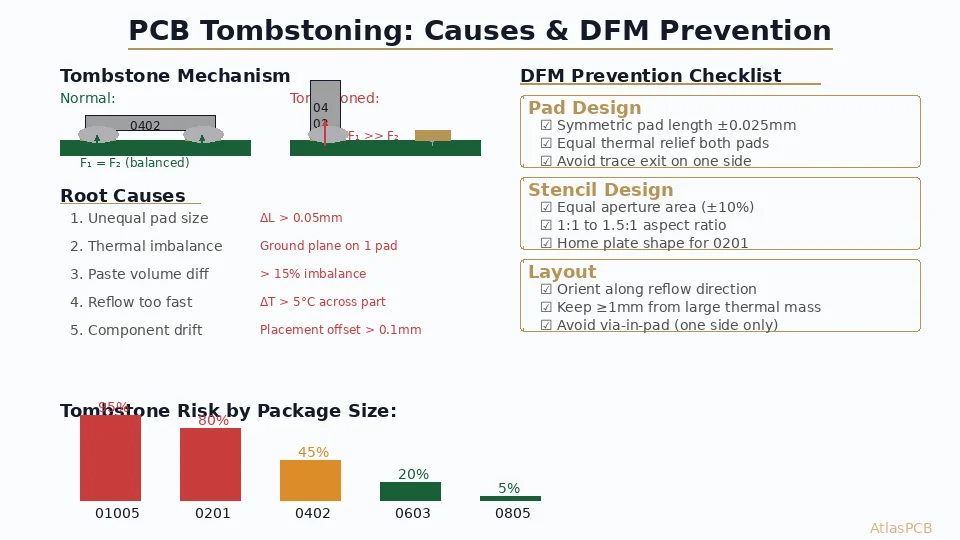
Tombstoning — also called the Manhattan effect, drawbridging, or Stonehenge effect — is one of the most persistent and frustrating defects in surface-mount assembly. The defect occurs when one end of a two-terminal chip component lifts vertically during reflow soldering, standing the component on its end like a tombstone. At best, it creates an open circuit. At worst, it passes visual inspection but creates an intermittent connection that fails in the field.
For high-reliability applications governed by IPC-A-610 Class 3, tombstoning is a reject condition with zero tolerance. Even in Class 2 consumer electronics, tombstoning rates above 50 DPM (defects per million) trigger process holds and root cause investigations. This guide provides the engineering knowledge to design tombstoning out of your PCB before it ever reaches the assembly line.
The Physics of Tombstoning
Understanding the root physics is essential for effective prevention. During reflow soldering, solder paste on both pads of a chip component melts and wets the metallized terminations. The molten solder exerts a surface tension force that pulls the component toward the pad — this is the self-centering force that makes SMT work.
Tombstoning occurs when the solder on one pad melts and generates a wetting force before the solder on the other pad melts. The one-sided force creates a torque around the component’s center of gravity that overcomes the restoring force of gravity and any remaining paste viscosity on the cooler pad.
The physics can be expressed as a simple torque balance:
τ_tombstone = F_surface_tension × d_arm
Where F_surface_tension is the wetting force of the molten solder (typically 0.5–2.0 mN for a 0402 component) and d_arm is the distance from the pivot point to the line of action (approximately half the component height, ~0.15mm for 0402).
The restoring gravitational torque is:
τ_gravity = m × g × d_cg
Where m is the component mass (~0.5 mg for 0402), g is gravitational acceleration, and d_cg is the horizontal distance from the pivot to the center of gravity (~0.3mm for 0402).
For a 0402 component: τ_tombstone ≈ 0.075 µN·mm while τ_gravity ≈ 0.0015 µN·mm. The surface tension torque is roughly 50× the gravitational restoring torque. This explains why even small imbalances in wetting timing lead to tombstoning — gravity alone cannot prevent it.
Root Causes: The Five Imbalance Factors
Every tombstoning incident can be traced to one or more of these five imbalance factors:
1. Pad Geometry Asymmetry
Unequal pad dimensions cause unequal solder paste volume and unequal wetting area. Per IPC-7351B, the land pattern for a chip component specifies identical pads with tolerances of ±0.05mm. In practice, pad asymmetry can result from:
- Design error: Manually drawn pads with different lengths or widths
- Gerber rounding: CAD tools rounding pad dimensions differently for the two pads
- Etch variation: Non-uniform copper etching creating slightly different pad sizes (typically ±10–15 µm)
A 0.1mm difference in pad length can increase tombstoning rates by 5–10× for 0201 components.
2. Thermal Imbalance
This is the single most common cause of tombstoning in well-designed boards. When one pad connects to a large copper area (ground plane, [thermal via array]/blog/pcb-thermal-via-design/), power pour) and the other pad connects to a thin trace, the thermal mass difference causes the trace-connected pad to reach reflow temperature first.
The temperature differential needed to cause tombstoning is surprisingly small:
| Component Size | Critical ΔT (between pads) |
|---|---|
| 01005 | 2–3°C |
| 0201 | 3–5°C |
| 0402 | 5–10°C |
| 0603 | 10–20°C |
| 0805 | > 25°C (rare) |
3. Solder Paste Volume Imbalance
IPC-7525 (Stencil Design Guidelines) specifies that solder paste volume should be consistent across all pads. A volume difference of > 15% between the two pads of a chip component significantly increases tombstoning risk. Volume imbalance can result from:
- Stencil aperture inconsistency: Different aperture sizes or aspect ratios
- Paste release variation: One aperture releasing more paste than the other due to aperture wall finish or stencil gasket issues
- Print offset: The entire stencil pattern shifted relative to pads, causing one pad to receive more paste than the other
4. Reflow Profile Issues
An aggressive ramp rate from soak to peak (> 3°C/sec) amplifies thermal gradients across the board. Boards with varying copper density create localized hot and cold spots. Without an adequate soak zone to equalize temperature, pads on the “hot” side of a temperature gradient melt first.
5. Component Placement Accuracy
Modern pick-and-place machines achieve ±25–50 µm placement accuracy, which is adequate for most components. However, for 01005 components (0.4mm × 0.2mm), even a 50 µm offset places the component significantly off-center, creating an asymmetric wetting condition.
PCB Design Strategies for Tombstoning Prevention
The most effective tombstoning prevention happens at the PCB design stage, long before assembly. Here are the critical design rules:
Pad Design per IPC-7351B
IPC-7351B defines three density levels for land patterns:
- Level A (Most): Maximum pad size — most manufacturing-robust, easiest to solder
- Level B (Nominal): Standard pad size — balanced routing density and solderability
- Level C (Least): Minimum pad size — highest routing density, most process-sensitive
For tombstoning prevention, Level A or B is strongly recommended for all chip components ≤ 0603. Level C patterns significantly increase tombstoning risk for small components.
Key pad geometry rules:
- Both pads identical: Length, width, and copper area must match within ±0.05mm
- Symmetric pad-to-trace routing: If a trace exits Pad 1 from the left side, route the trace from Pad 2 from the right side — maintain thermal symmetry
- No asymmetric copper features: Do not place a via-in-pad on one pad and not the other. If [via-in-pad]/blog/pcb-via-types-guide/) is needed, use it on both pads or neither
- Equal solder mask openings: Solder mask openings (NSMD or SMD type) must be identical for both pads

Thermal Balancing Techniques
Thermal imbalance is the primary design-controllable cause of tombstoning. The following techniques equalize thermal paths:
Thermal Relief on Both Pads
When one pad of a chip component connects to a copper pour or plane, both pads should use thermal relief patterns — even if the second pad connects only to a trace. This ensures both pads have similar thermal resistance to the surrounding copper.
Standard thermal relief parameters per IPC-7351B:
- Spoke width: 0.2–0.3mm
- Spoke count: 2 or 4 (use same count on both pads)
- Gap width: 0.2–0.3mm
- Anti-pad diameter: Pad diameter + 0.5mm minimum
Copper Thieving
Add small copper pads (non-functional “thermal thieving” pads) near the trace-connected pad to increase its local thermal mass. The thieving copper should be placed within 0.5mm of the pad and connected by a short trace of ≥0.2mm width. This is especially effective for 0201 components near large ground pours.
Trace Width Matching
If the traces connecting to both pads differ significantly in width or length, the wider/shorter trace conducts more heat to its pad. Aim for trace widths within 50% of each other for the first 1mm of routing from each pad. For [impedance-controlled traces]/blog/pcb-impedance-control/) where width is fixed, add thermal relief to compensate.
Via Placement Symmetry
Vias near component pads act as thermal conduits to inner layers. A via placed 0.3mm from one pad but 2mm from the other creates significant thermal asymmetry. Rule: any via within 1mm of a chip component pad should have a corresponding via at equal distance from the opposite pad, or thermal relief should be added to compensate.
Component Orientation Guidelines
Orienting chip components correctly relative to the reflow conveyor direction and board thermal gradients can reduce tombstoning risk:
- Preferred orientation: Component long axis perpendicular to the reflow conveyor direction. This ensures both pads enter the peak temperature zone simultaneously.
- Avoid hot-spot alignment: Do not place chip components with one pad over a thermal via array and the other pad over bare laminate. Check the [thermal management]/blog/pcb-thermal-management/) layout for hot spots.
- Wave solder orientation: For mixed-technology boards with wave soldering, orient components parallel to the wave direction so both pads contact the solder wave simultaneously.
Stencil Design per IPC-7525
The solder paste stencil is the primary tool for controlling paste volume. IPC-7525 provides guidelines for stencil aperture design that directly impact tombstoning:
Aperture Size Rules
- Area ratio: Aperture area / wall area should be ≥ 0.66 for laser-cut stainless steel stencils (≥ 0.60 for electroformed nickel stencils). Below these ratios, paste release becomes unreliable.
- Aperture width: ≥ 4× stencil thickness for reliable release. For a 0.1mm (4 mil) thick stencil, minimum aperture width = 0.4mm.
- Both apertures identical: Aperture dimensions for both pads of a chip component must be identical. Any asymmetry directly translates to paste volume asymmetry.
Stencil Thickness Selection
| Component Size | Recommended Stencil Thickness |
|---|---|
| 01005 | 0.060–0.080mm (2.4–3 mil) |
| 0201 | 0.080–0.100mm (3–4 mil) |
| 0402 | 0.100–0.125mm (4–5 mil) |
| 0603 | 0.125–0.150mm (5–6 mil) |
| 0805+ | 0.125–0.200mm (5–8 mil) |
For boards with mixed component sizes, step-down stencils (locally reduced thickness over small-pad areas) can optimize paste volume for each component size.
Aperture Modifications for Tombstoning-Prone Areas
For components in known high-risk locations (adjacent to ground planes, near board edges, etc.), aperture reduction of 5–10% on both pads can reduce tombstoning by decreasing the absolute surface tension force. However, this must be balanced against insufficient solder volume (causing dry joints or HIP — head-in-pillow defects).
Reflow Profile Optimization
The reflow profile is the final process variable affecting tombstoning. An optimized profile equalizes temperature across the board before the solder reaches liquidus.
Profile Zones and Their Impact on Tombstoning
Preheat Zone (25°C → 150°C)
- Ramp rate: 1.0–2.5°C/sec (per IPC-7530 reflow guidelines)
- Purpose: Activate flux, evaporate solvents
- Tombstoning impact: Minimal, as solder is still solid
Soak Zone (150°C → 200°C)
- Duration: 60–120 seconds
- Purpose: Equalize temperature across the board — this is the critical zone for tombstoning prevention
- Target: Temperature delta across the board ΔT < 5°C at end of soak
- Tombstoning impact: High. An inadequate soak zone is the #1 reflow-related cause of tombstoning
Reflow Zone (200°C → peak → 200°C)
- Time above liquidus (TAL): 45–90 seconds for SAC305 (liquidus 217°C)
- Peak temperature: 235–250°C
- Ramp to peak: ≤ 3°C/sec (slower is better for tombstoning prevention)
- Tombstoning impact: The ramp-to-peak rate determines how quickly thermal gradients develop. Slower ramps give the soak zone more time to work.
Cooling Zone
- Cooling rate: 2–4°C/sec
- Tombstoning impact: Minimal (solder is already solidified)
Nitrogen Atmosphere
Reflow in nitrogen atmosphere (< 500 ppm O2) improves solder wetting uniformity and reduces tombstoning rates by 30–50% compared to air reflow. The improved wetting means both pads reach full wetting force more quickly, reducing the time window for imbalanced forces. For high-density designs with 0201/01005 components, nitrogen reflow is strongly recommended.
Component-Specific Challenges
0201 Components (0.6mm × 0.3mm)
0201 is the current mainstream ultra-miniature size and is highly susceptible to tombstoning:
- Component mass: ~0.5 mg (gravitational restoring force is negligible)
- Typical tombstoning rate in optimized process: 5–20 DPM
- Critical design rules:
- Pad tolerance: ≤ 0.03mm (stricter than IPC-7351B general requirement)
- Trace exit direction: Must be symmetric
- No copper pour connection without thermal relief on both pads
- Recommended [surface finish]/blog/pcb-surface-finish-comparison-2026/): ENIG or immersion tin (flat surfaces improve paste release consistency)
01005 Components (0.4mm × 0.2mm)
01005 is the smallest standard chip component and represents the extreme challenge for tombstoning prevention:
- Component mass: ~0.15 mg
- Typical tombstoning rate in optimized process: 20–100 DPM
- Additional requirements:
- Stencil: Electroformed nickel, 0.060mm thickness
- Placement accuracy: ±15 µm required
- Pad geometry: Must be derived from validated library (no manual pad creation)
- Reflow: Nitrogen atmosphere mandatory
- 100% AOI (Automated Optical Inspection) required for this component size
DFM Checks for Tombstoning Risk
Before releasing a design for production, run these DFM checks on every chip component ≤ 0603:
Check 1: Pad Symmetry Verification
- Compare both pad dimensions: ΔLength ≤ 0.05mm, ΔWidth ≤ 0.05mm
- Compare solder mask opening dimensions
- Verify pad corner radii match (if radiused)
Check 2: Thermal Symmetry Analysis
- Identify all chip components with one pad on a copper pour and one pad on a trace
- Flag components where pad-connected copper area differs by > 3× between pads
- Verify thermal relief patterns are symmetric
Check 3: Via Proximity Check
- Flag any via within 0.5mm of a chip component pad that does not have a symmetric counterpart
- Verify [via-in-pad]/blog/pcb-via-types-guide/) usage is symmetric (both pads or neither)
Check 4: Component Orientation
- Verify components are oriented with long axis perpendicular to expected reflow conveyor direction
- Flag components with pads straddling thermal boundaries (e.g., one pad over ground plane, one pad over signal layer void)
Check 5: Stencil Design Review
- Verify aperture dimensions match pad dimensions (or approved reduction percentages)
- Calculate area ratio for each aperture: must be ≥ 0.66
- Verify step-down areas (if any) provide adequate coverage
Most modern DFM tools (Valor NPI, DFMStream, CAM350) include automated tombstoning risk analysis. At Atlas PCB, our engineering review process includes tombstoning risk assessment as part of every DFM check.
Process Monitoring and Defect Tracking
Even with optimized design and process, ongoing monitoring is essential:
Key Process Indicators (KPIs) for Tombstoning
- Tombstoning rate by component size: Track separately for each size (0201, 0402, 0603)
- Tombstoning rate by board location: Identifies thermal hot spots or stencil issues
- Tombstoning rate vs. reflow profile: Correlate with profile changes
- Tombstoning rate vs. paste lot: Identifies paste consistency issues
Industry Benchmarks
| Process Maturity | 0201 Tombstoning Rate | 0402 Tombstoning Rate |
|---|---|---|
| World-class | < 5 DPM | < 1 DPM |
| Good | 5–20 DPM | 1–5 DPM |
| Acceptable | 20–50 DPM | 5–20 DPM |
| Needs improvement | > 50 DPM | > 20 DPM |
Conclusion
Tombstoning is a defect that is far easier to prevent than to correct after the fact. The most effective approach combines symmetric pad design per IPC-7351B, thermal balancing through deliberate copper and via management, consistent solder paste deposition per IPC-7525 stencil guidelines, and optimized reflow profiles with adequate soak zones.
For engineers designing with 0201 and 01005 components, tombstoning prevention must be a first-order design consideration — not an afterthought caught during production DFM review. By incorporating the design rules and DFM checks outlined in this guide, you can achieve tombstoning rates well below 20 DPM even for the most challenging component sizes.
The cost of prevention is negligible compared to the cost of rework, scrap, and field failures caused by intermittent tombstone-related open circuits. When your [multilayer PCB manufacturing]/blog/multilayer-pcb-manufacturing-process-explained/) partner offers DFM review as part of the quoting process, take advantage of it — tombstoning risk assessment should be standard practice.
Ready to start your project? Upload your Gerbers for a free engineering review, or talk to an engineer about your design requirements.
Further Reading
- [Via-in-Pad Design: Filled, Capped, and Plated Over — Complete Guide]/blog/via-in-pad-design/)
- [PCB DFM Checklist: 50 Points to Review Before Sending Gerbers]/blog/pcb-dfm-checklist/)
- [PCB Manufacturer with Engineering Review: Why Human DFM Audit Matters]/blog/pcb-manufacturer-engineering-review/)
- [ENEPIG vs ENIG: Which PCB Surface Finish for Your Design?]/blog/enepig-vs-enig/)
- [PCB Surface Finish Guide: HASL, ENIG, OSP and More Compared]/blog/pcb-surface-finish-guide/)
About AtlasPCB — We specialize in complex PCB manufacturing for HDI, RF, and high-reliability applications. Explore our PCB assembly services, or get an free engineering DFM review . Every order includes free engineering review. Get your quote.
Reviewed by AtlasPCB Engineering Team — IPC-certified manufacturing specialists with 15+ years of production experience in HDI, RF, and high-reliability PCB fabrication. Content based on factory floor data and real customer design reviews.
- tombstoning
- smt-assembly
- reflow-soldering
- dfm