· AtlasPCB Engineering · Engineering · 6 min read
ENIG vs ENEPIG Surface Finish: Complete Selection Guide for PCB Assembly
Learn when to choose ENIG or ENEPIG surface finish for your PCB. Compare cost, reliability, wire bonding compatibility, and black pad risk. Engineering decision framework included.
Understanding PCB Surface Finishes: Why ENIG and ENEPIG Dominate
Selecting the right surface finish is one of the most consequential decisions in PCB design. The finish protects exposed copper from oxidation, ensures reliable solder joints, and determines which assembly technologies are compatible with your board. Among the dozen-plus finishes available, ENIG and ENEPIG have emerged as the dominant choices for modern electronics—together accounting for over 60% of all PCB production in high-reliability segments.
This guide provides the engineering framework to choose between them, with real-world data on cost, reliability, and manufacturing considerations.
ENIG: The Industry Workhorse
Process and Structure
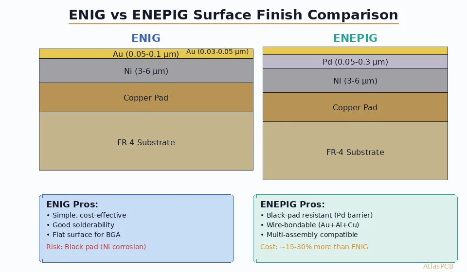
ENIG (Electroless Nickel Immersion Gold) deposits two layers onto copper pads through a chemical (autocatalytic) process:
- Electroless Nickel (EN): 3–6 µm thickness, 7–9% phosphorus content
- Immersion Gold (IG): 0.05–0.1 µm (2–4 microinches)
The nickel layer serves as a barrier between copper and the solderable surface, while the thin gold prevents nickel oxidation during storage. During soldering, the gold dissolves into the solder and the actual intermetallic compound (IMC) forms between tin and nickel.
ENIG Advantages
- Excellent coplanarity: ±5 µm flatness across the board—critical for fine-pitch BGA
- Long shelf life: 12+ months storage with proper packaging
- Lead-free compatible: Works with SAC305 and all modern alloys
- Contact surface: Suitable for membrane switches, press-fit connectors, and test points
- Cost-effective: $0.03–0.06/cm² premium over HASL
ENIG Limitations
The primary concern with ENIG is the black pad phenomenon—a corrosion attack on the nickel layer during gold deposition that creates brittle, unreliable solder joints. Black pad occurs at rates of 1–5% in production, is invisible during visual inspection, and typically manifests as field failures months or years after assembly.
Other limitations include:
- Not suitable for wire bonding
- Signal loss at RF frequencies (nickel is ferromagnetic)
- Aluminum wire bonds are unreliable
ENEPIG: The Universal Finish
Process and Structure
ENEPIG adds a palladium interlayer, creating a three-metal stack:
- Electroless Nickel (EN): 3–6 µm, 7–9% phosphorus
- Electroless Palladium (EP): 0.05–0.3 µm
- Immersion Gold (IG): 0.03–0.05 µm
The palladium layer fundamentally changes the chemistry: gold deposits onto palladium rather than attacking nickel, eliminating the corrosion mechanism that causes black pad.
ENEPIG Advantages
- Zero black pad risk: Palladium barrier prevents nickel corrosion during gold deposition
- Universal wire bonding: Compatible with gold, aluminum, and copper wire bonding
- Mixed-assembly compatible: Single finish supports SMT, through-hole, wire bonding, and press-fit
- Superior shelf life: Palladium oxidation resistance extends usable life to 18+ months
- Better RF performance: Thinner nickel exposure reduces magnetic loss at GHz frequencies
ENEPIG Limitations
- Cost premium: 15–30% more than ENIG ($0.05–0.09/cm² over HASL)
- Process complexity: Additional bath requires tighter process control
- Fewer qualified suppliers: Not all fabricators offer reliable ENEPIG
- Palladium embrittlement risk: Excessive palladium (>0.3 µm) can cause solder joint brittleness
Head-to-Head Comparison
| Parameter | ENIG | ENEPIG |
|---|---|---|
| Layer structure | Ni + Au | Ni + Pd + Au |
| Typical cost premium | $0.03–0.06/cm² | $0.05–0.09/cm² |
| Black pad risk | 1–5% occurrence | Eliminated |
| Gold wire bonding | No | Yes |
| Aluminum wire bonding | Marginal | Yes |
| Copper wire bonding | No | Yes |
| Shelf life | 12 months | 18+ months |
| BGA compatibility | Excellent | Excellent |
| RF performance | Good (Ni loss at >6 GHz) | Better (less Ni exposure) |
| Press-fit compatible | Yes | Yes |
| IPC-4556 compliant | N/A (IPC-4552) | Yes |
PCB Surface Finish Expertise
Need Help Choosing ENIG or ENEPIG?
Our engineers review your BOM and assembly requirements to recommend the optimal surface finish—free DFM consultation included.
Get Engineering Review →Engineering Decision Framework
Choose ENIG When:
- Budget-constrained consumer electronics where 1–5% black pad risk is acceptable given warranty cost models
- Standard SMT-only assembly with no wire bonding requirements
- Large production volumes where the 15–30% cost difference across millions of pads is significant
- Existing qualified process at your CM that reliably controls nickel phosphorus content (>9% P)
Choose ENEPIG When:
- Wire bonding is required—gold wire, aluminum wire, or copper wire to any pad
- Mixed-technology boards combining SMT + wire bonding + press-fit on one PCB
- Zero-defect requirements—medical, aerospace, automotive safety systems
- Fine-pitch BGA (≤0.4 mm pitch) where individual joint reliability is critical
- Multi-step assembly where boards undergo multiple reflow cycles
- RF/microwave circuits operating above 6 GHz where nickel magnetic loss matters
The Black Pad Decision
If your product’s field failure cost exceeds $100 per unit (including recall, repair, reputation), the math almost always favors ENEPIG. At $0.02/pad premium on a 500-pad board, ENEPIG adds $10—trivial compared to a single field return.
For consumer IoT devices selling at $15 with disposable economics, ENIG’s cost advantage wins if your fabricator maintains tight process control.
Specification Tips for Fabrication
ENIG (per IPC-4552B):
Nickel thickness: 3.0–6.0 µm
Nickel phosphorus content: 7–9 wt% (mid-phos)
Gold thickness: 0.05–0.10 µm (2–4 µin)
Nickel crystal structure: Amorphous (required for corrosion resistance)
ENEPIG (per IPC-4556A):
Nickel thickness: 3.0–6.0 µm
Nickel phosphorus content: 7–9 wt%
Palladium thickness: 0.05–0.15 µm (for solder-only)
                     0.15–0.30 µm (for wire bonding)
Gold thickness: 0.03–0.05 µm
Critical note: Specify palladium thickness based on your assembly method. Wire bonding requires the thicker range (≥0.15 µm), but exceeding 0.3 µm risks palladium embrittlement in solder joints.
Manufacturing and Quality Control
ENIG Process Control
The primary failure mode—black pad—is controlled through:
- Phosphorus content: Maintain 8–9% (higher P = more corrosion resistant but harder to solder)
- Gold deposition rate: Slower is better—aggressive baths attack nickel faster
- Bath loading: Monitor nickel concentration and pH continuously
- IPC-4552B compliance testing: Cross-section SEM/EDX on coupon every lot
ENEPIG Process Control
Additional considerations for the palladium step:
- Bath stability: Palladium baths are less stable than nickel—monitor reducing agent concentration
- Deposition uniformity: Pd thickness variation should be <20% across the board
- No skip plating: Verify all pads receive palladium (missing Pd = same as ENIG risk)
- Contamination testing: ICP-OES verification of Pd purity
Soldering Performance Comparison
Both finishes provide excellent solderability with lead-free alloys. Key differences emerge in multi-reflow scenarios:
| Scenario | ENIG | ENEPIG |
|---|---|---|
| Single reflow (top-side SMT) | Excellent | Excellent |
| Double reflow (top + bottom SMT) | Good | Excellent |
| Triple reflow (+ rework) | Risk increases | Reliable |
| Wave solder (through-hole) | Good | Good |
| Mixed SMT + wave | Good | Excellent |
The palladium layer in ENEPIG provides additional solder wetting margin after multiple thermal excursions, making it superior for complex assembly sequences.
Industry Trends and Future Outlook
The ENEPIG adoption curve is accelerating:
- Automotive electronics: IATF 16949 quality requirements increasingly mandate ENEPIG for safety-critical ECUs
- 5G infrastructure: RF performance benefits drive adoption in antenna and amplifier boards
- Advanced packaging: Fan-out wafer-level packaging (FOWLP) and system-in-package (SiP) prefer ENEPIG for mixed interconnect
- Cost convergence: As ENEPIG volume grows, the price premium over ENIG is decreasing (was 40%+ in 2020, now 15–30%)
For new designs entering production in 2026+, ENEPIG should be the default consideration unless cost pressure explicitly requires ENIG.
Conclusion
The ENIG vs ENEPIG decision fundamentally comes down to risk tolerance vs cost. ENIG remains a reliable, cost-effective finish for standard SMT assembly when process control is tight. ENEPIG eliminates black pad risk entirely and adds wire bonding capability at a modest premium.
For engineers designing products where field failure carries significant cost—medical devices, automotive safety systems, aerospace electronics, or high-reliability industrial equipment—ENEPIG is the rational choice. The palladium barrier transforms an inherently risky chemical process (immersion gold attacking nickel) into a stable, predictable stack.
Ready to specify your surface finish? AtlasPCB offers both ENIG and ENEPIG with IPC-4552B/4556A certification. Our process engineers can review your design and recommend the optimal finish based on your assembly method, reliability requirements, and budget. Request a free DFM review →
Further Reading
About AtlasPCB — We specialize in complex PCB manufacturing for HDI, RF, and high-reliability applications. Explore our HDI PCB manufacturing capabilities, RF and high-frequency PCB services, or get an PCB assembly services . Every order includes free engineering review. Get your quote.
Reviewed by AtlasPCB Engineering Team — IPC-certified manufacturing specialists with 15+ years of production experience in HDI, RF, and high-reliability PCB fabrication. Content based on factory floor data and real customer design reviews.
- ENIG
- ENEPIG
- surface finish
- PCB assembly
- wire bonding
- black pad
- BGA
- soldering
- gold plating