· AtlasPCB Engineering · Engineering · 8 min read
PCB Tombstoning: Causes, Prevention & DFM Design Checklist
Engineering-focused guide to eliminating tombstoning defects through PCB design. Covers root cause physics, pad geometry rules, thermal balancing, stencil optimization, and a complete DFM checklist for 0201 and 01005 components.
Understanding Tombstoning Physics
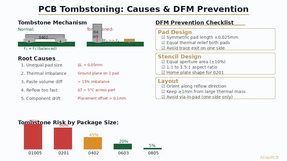
Tombstoning (also called the Manhattan effect or drawbridge defect) occurs when one end of a chip component lifts vertically during reflow soldering, resembling a tombstone standing upright. This defect is unique to passive chip components—resistors, capacitors, and inductors in packages from 0201 to 0805.
The physics are straightforward: during reflow, solder paste transitions to liquid state and surface tension forces pull the component toward the larger solder volume. If one pad’s solder melts before the other, or if the solder volumes are unequal, the resulting force imbalance rotates the component around its center of gravity.
The critical force equation:
F_lift = γ × L × cos(θ) × A_wet

Where:
γ = solder surface tension (~500 mN/m for SAC305 at 240°C)
L = wetted perimeter
θ = contact angle
A_wet = wetted area on the lifted pad
A force difference of just 0.5 mN between pads is sufficient to tombstone a 0201 component (mass: 0.15mg). This makes tombstoning one of the most sensitive defects to design asymmetry.
Root Causes of Tombstoning
1. Pad Geometry Asymmetry
The most common design-related cause. Any dimensional difference between the two pads creates unequal wetting area:
| Asymmetry Type | Risk Increase | Threshold |
|---|---|---|
| Pad length difference | 300% per 0.05mm | >0.025mm |
| Pad width difference | 150% per 0.05mm | >0.05mm |
| Solder mask opening mismatch | 200% per 0.05mm | >0.03mm |
| Trace exit asymmetry | 100% | Any one-sided exit |
2. Thermal Mass Imbalance
When one pad connects to a ground plane or large copper pour while the other connects to a thin trace, heat dissipation differs dramatically:
- Ground plane pad: Absorbs heat → solder melts later → lower wetting force initially
- Isolated pad: Reaches liquidus first → surface tension pulls component early
- Temperature differential >5°C across the component causes sequential melting
3. Solder Paste Volume Asymmetry
Unequal paste deposits create unequal solder volumes after reflow:
- Stencil aperture area difference >10% = high tombstone risk
- Paste printing offset >25% of pad width = unequal coverage
- Clogged stencil apertures = reduced paste on one pad
4. Component Placement Offset
Pick-and-place accuracy matters:
- Placement offset >50% of pad width shifts solder force balance
- Rotational offset >2° on fine-pitch components creates asymmetry
- Component arrives after paste begins melting (dual-pass reflow issue)
5. Reflow Profile Issues
- Fast ramp rate (>3°C/sec) creates temperature gradients across the board
- Short soak zone (<60 seconds) doesn’t equalize temperature
- Peak temperature too high reduces solder viscosity excessively
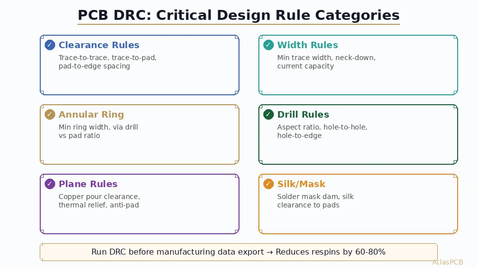
DFM Prevention Checklist
Pad Design Rules (IPC-7351B Compliance)
For each passive component:
☑ Both pads identical dimensions — length and width within ±0.025mm ☑ Identical solder mask openings — NSMD or SMD, same on both sides ☑ Symmetric trace routing — if trace exits one pad, add dummy trace on other ☑ Equal thermal relief — same spoke pattern and gap on both pads ☑ No via-in-pad on only one side — either both or neither ☑ Consistent copper fill — both pads have same surrounding copper density
Recommended Pad Geometries by Package
| Package | Pad Length | Pad Width | Gap | Stencil Aperture |
|---|---|---|---|---|
| 01005 | 0.25mm | 0.20mm | 0.20mm | 0.20×0.15mm |
| 0201 | 0.35mm | 0.30mm | 0.30mm | 0.28×0.25mm |
| 0402 | 0.55mm | 0.50mm | 0.50mm | 0.45×0.45mm |
| 0603 | 0.80mm | 0.75mm | 0.80mm | 0.65×0.65mm |
| 0805 | 1.00mm | 1.20mm | 1.00mm | 0.85×1.10mm |
Thermal Balancing Techniques
When one pad must connect to a large copper area:
- Add thermal relief on both pads — even if one pad doesn’t need it for manufacturability
- Equalize connected copper area — add a dummy copper shape on the isolated pad
- Use thermal vias symmetrically — if one pad has [thermal vias]/blog/pcb-thermal-via-design/), add matching vias under the other pad
- Split ground plane locally — create a slotted plane reducing thermal conductivity to one pad
🔧 Need Tombstone-Free PCB Assembly?
AtlasPCB's DFM review checks every passive component for pad symmetry, thermal balance, and stencil optimization before manufacturing. We catch tombstoning risks at the design stage.
Get Your Free DFM Review →Stencil Design Optimization
The stencil is your primary paste volume control:
Aperture sizing rules:
- Equal area on both pads (within ±5% for 0201 and below)
- Aspect ratio (width/thickness): ≥1.5 for reliable paste release
- Area ratio (aperture area / wall area): ≥0.66 for consistent transfer
Advanced stencil techniques for tombstone prevention:
- Home plate apertures — Pentagon shape on 0201/01005 reduces paste volume while maintaining print definition
- Rounded corners — Radius on aperture corners improves paste release consistency
- Stepped stencil — Thinner locally (75μm vs. 100μm) for small components reduces excess paste
- Nano-coating — Hydrophobic stencil coating ensures consistent paste release
Layout and Orientation Rules
Component placement on the PCB layout matters:
☑ Orient components along reflow wave — Longer axis parallel to conveyor direction ☑ Keep 1mm minimum from large thermal masses — Transformers, heatsinks, large connectors ☑ Avoid clustering small and large components — Temperature gradients between neighbors ☑ Consistent ground pour proximity — If one component is near pour, route others similarly ☑ No mechanical stress during reflow — Ensure flat board support in reflow zone
Via-in-Pad Considerations
Via-in-pad creates solder volume loss on the viaed pad:
- Unfilled via-in-pad on one side — Solder wicks down via, reducing joint volume → HIGH tombstone risk
- Both pads with filled/capped vias — Acceptable, symmetric condition
- One pad via-in-pad, other pad no via — UNACCEPTABLE for 0402 and smaller
If via-in-pad is required for routing density, use [via-in-pad plated over (VIPPO)]/blog/pcb-via-in-pad-plated-over-design/) with copper fill and planarization to create a flat, solderable surface identical to a standard pad.
Process-Level Controls
While this article focuses on DFM design decisions, process parameters significantly influence tombstoning rates:
Reflow Profile Optimization
For tombstone-sensitive boards (0201/01005 heavy):
Preheat ramp:     1.0-1.5°C/sec (slower = better temperature equalization)
Soak zone:        150-200°C for 90-120 seconds
Soak ΔT:         <5°C across board surface
Ramp to peak:    1.0-2.0°C/sec through liquidus
Peak temperature: 235-245°C for SAC305
Time above liquidus: 45-75 seconds
Cooling rate:     <3°C/sec (prevent thermal shock)
Nitrogen Atmosphere Benefits
Reflow in nitrogen (<1000 PPM O₂) reduces tombstoning by:
- Preventing oxide formation on pad surfaces → better wetting → simultaneous melting
- Reducing flux consumption → more uniform flux activation
- Enabling lower peak temperatures → less thermal stress
- Typical tombstoning reduction: 40-60% with nitrogen vs. air reflow
Component Placement Accuracy
For modern [SMT pad design]/blog/pcb-smt-pad-design-fine-pitch/):
- Placement accuracy requirement: ±0.025mm for 01005, ±0.05mm for 0201
- Rotational accuracy: <1° for 01005, <2° for 0201
- Force control: 0.1-0.5N placement force (avoid paste displacement)
- Nozzle selection: Component-specific vacuum nozzles for consistent pickup
Tombstoning Risk Assessment by Design Feature
| Design Feature | Risk Level | Mitigation |
|---|---|---|
| 01005 components | Very High (95%) | Full DFM optimization required |
| 0201 components | High (80%) | Thermal balancing + stencil optimization |
| 0402 on ground plane | Medium (45%) | Thermal relief + symmetric routing |
| 0603 standard layout | Low (20%) | Standard IPC-7351B pads sufficient |
| 0805 components | Very Low (5%) | Rarely tombstones, weight provides stability |
| Via-in-pad (one side) | High (75%) | Fill and cap both pads |
| Trace exit asymmetry | Medium (40%) | Add dummy trace or thermal spoke |
| Near large connector | Medium (50%) | Increase spacing to >2mm |
Common DFM Mistakes That Cause Tombstoning
Mistake 1: Different Pad Shapes in Library
Many EDA libraries have footprints where one pad is rectangular and the other has a slightly different shape (due to pin 1 identification or thermal pad integration). Always verify both pads are geometrically identical in your footprint library.
Mistake 2: Copper Pour Too Close on One Side
Automatic copper pour algorithms may fill closer to one pad than the other. Always set consistent pour-to-pad clearance and verify symmetry after polygon regeneration.
Mistake 3: Solder Mask Registration Assumption
If solder mask misregisters by 25μm (normal fabrication tolerance), asymmetric [solder mask openings]/blog/pcb-solder-mask-dam-design-rules-dfm/) on the two pads will expose different copper areas. Design mask openings with tolerance in mind.
Mistake 4: Routing Traces from Only One Pad
When a resistor in series requires traces on both ends, ensure both traces exit at the same angle and width. A wide trace (0.2mm) exiting one pad and a narrow trace (0.1mm) from the other creates thermal asymmetry.
Mistake 5: Ignoring Board Edge Effects
Components near the board edge reach reflow temperature faster than those in the center. If a 0201 component is placed at the board edge with one pad facing the edge, the outer pad heats first—creating sequential melting.
Inspection and Detection
After assembly, tombstoning is detected by:
- [AOI (Automated Optical Inspection)]/blog/aoi-spi-inspection-pcb-assembly-quality-control/): Detects lifted components via shadow analysis and height profiling
- SPI (Solder Paste Inspection): Pre-reflow detection of paste volume asymmetry (predictive)
- X-ray: Verifies solder joint integrity for partially tombstoned components (lifted but not vertical)
- Visual inspection: Obvious for fully tombstoned parts
SPI as Predictive Quality Control
Solder paste inspection before reflow can predict tombstoning:
- Volume difference >15% between pads → flag for rework before reflow
- Height difference >10μm → potential tombstone candidate
- Offset >25% of pad width → placement correction needed
Industry Statistics and Benchmarks
Based on IPC assembly benchmark data:
- Standard process (no DFM optimization): 500-2000 PPM tombstoning for 0201
- DFM-optimized design: 50-100 PPM tombstoning for 0201
- Full process optimization (N₂ + DFM + SPI): <20 PPM tombstoning for 0201
- Cost of tombstoning defect: $2-15 per component (rework labor + risk of pad damage)
Conclusion
Tombstoning is fundamentally a design-preventable defect. While process controls (reflow profile, nitrogen, placement accuracy) provide additional margin, the DFM design decisions—pad symmetry, thermal balancing, stencil aperture design, and component placement—determine whether tombstoning is even possible.
For designs using 0402 and smaller components, perform a specific tombstoning DFM review checking every passive component against the checklist above. The cost of prevention (engineering time at design phase) is orders of magnitude less than the cost of post-assembly rework.
Further Reading
- [PCB Tombstoning Prevention: SMT Process Guide]/blog/pcb-tombstoning-prevention-smt/) — Detailed process optimization for reflow
- [Common PCB Defects & Prevention]/blog/common-pcb-defects-prevention/) — Overview of all major assembly defects
- [PCB Solder Paste Stencil Design]/blog/pcb-solder-paste-stencil-design/) — Stencil engineering for consistent printing
- [SMT Pad Design for Fine-Pitch]/blog/pcb-smt-pad-design-fine-pitch/) — Advanced pad geometries
- [AOI & SPI Inspection Quality Control]/blog/aoi-spi-inspection-pcb-assembly-quality-control/) — Post-assembly verification methods
About AtlasPCB — We specialize in complex PCB manufacturing for HDI, RF, and high-reliability applications. Explore our PCB assembly services, or get an free engineering DFM review . Every order includes free engineering review. Get your quote.
Reviewed by AtlasPCB Engineering Team — IPC-certified manufacturing specialists with 15+ years of production experience in HDI, RF, and high-reliability PCB fabrication. Content based on factory floor data and real customer design reviews.
- tombstoning
- dfm
- smt-design
- chip-components
- reflow-soldering