· AtlasPCB Engineering · Engineering · 9 min read
Mixed-Signal PCB Layout: Grounding, Partition Strategies, and Noise Isolation for ADC/DAC Systems
Master mixed-signal PCB design with proven partition strategies, single-point grounding, guard traces, and analog-digital isolation techniques for high-resolution ADC/DAC applications.

Why Mixed-Signal Layout Demands Special Attention
Every modern electronic system is mixed-signal. Whether you are designing a data acquisition module, a medical imaging front-end, or an IoT sensor node, your PCB contains both precision analog circuits (amplifiers, filters, converters) and noisy digital logic (microcontrollers, FPGAs, communication interfaces). The challenge is coexisting: digital circuits switch milliamps in nanoseconds, generating broadband noise that can destroy the microvolt-level sensitivity your analog section requires.
A poorly laid out mixed-signal board can lose 20–30 dB of achievable dynamic range — turning a 16-bit ADC into a 12-bit one in practice. Conversely, a disciplined layout can achieve converter performance within 1–2 LSB of the datasheet specification.
This guide covers the proven layout strategies used by experienced PCB designers to achieve maximum analog performance alongside digital functionality, without resorting to exotic (and expensive) board constructions.
The Ground Plane Debate: Split vs. Unified
The Old Approach: Split Ground Planes
In the 1990s, application notes universally recommended physically splitting the ground plane into AGND and DGND regions. The logic seemed sound: prevent noisy digital return currents from flowing through the analog ground region.
However, split planes create more problems than they solve:
- Increased loop area — signals crossing the split must detour around the gap, creating large current loops that act as antennas
- Impedance discontinuities — traces crossing a plane gap see a sudden impedance spike, causing reflections
- Slot antenna effects — the split itself radiates and receives electromagnetic energy
- Resonances — narrow bridge connections between split regions can resonate at frequencies within your signal bandwidth
The Modern Approach: Unified Ground with Discipline
Current best practice (endorsed by TI, Analog Devices, and Linear Technology application notes since approximately 2005) is to use a single, solid, unbroken ground plane and control current flow through intelligent component placement and routing.
The principle: ground current returns directly beneath the signal trace that generated it. If you keep analog signals physically separated from digital signals, their return currents automatically stay separated on the ground plane — no split required.
When Splitting Is Still Appropriate
There are specific cases where a controlled split remains valid:
- Data converter datasheets that explicitly mandate it (becoming rare)
- Extreme high-voltage isolation (safety requirement, not noise)
- Mixed power domains requiring galvanic isolation (optocoupler/isolated DC-DC boundaries)
Even in these cases, the split should be bridged at one — and only one — carefully chosen point.
Component Placement: The Foundation of Mixed-Signal Success
Layout success is 70% placement. Get placement right, and routing becomes straightforward. Get it wrong, and no amount of routing cleverness will save you.
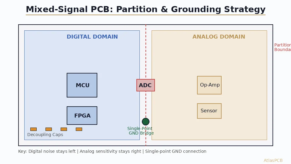
The Partition Strategy
Divide your board into functional zones:
| Zone | Components | Characteristics |
|---|---|---|
| Digital Core | MCU, FPGA, RAM, flash, USB/Ethernet PHY | High di/dt, fast edges, tolerant of noise |
| Analog Front-End | Op-amps, instrumentation amps, references, filters | Low-level signals, high sensitivity |
| Converter Bridge | ADC, DAC, codec | Straddles both domains |
| Power | Regulators, inductors, bulk caps | Switching noise source |
| I/O Connectors | External interfaces | EMI entry/exit point |
Placement Rules
- Place the ADC/DAC at the domain boundary — analog inputs face analog components, digital outputs face digital components
- Keep crystal oscillators and PLLs on the digital side, as far from analog inputs as board constraints allow
- Group analog signal chain components in a logical flow: connector → filter → amplifier → ADC
- Place power supply switching regulators on the opposite side of the board from sensitive analog circuits, or at minimum 30 mm away
- Position the voltage reference close to the ADC VREF pin, away from digital switching noise
Need Expert Mixed-Signal PCB Layout?
AtlasPCB's engineering team reviews DFM and signal integrity for mixed-signal boards — from 16-bit data acquisition to medical imaging front-ends.
Request DFM Review →Grounding Architecture: Single-Point Connection
The Star Ground Concept
For mixed-signal boards, implement a star ground topology at the system level:
- All ground connections radiate from a single, central point (typically the ADC ground pins)
- Analog ground currents and digital ground currents both return to this star point but via different physical paths on the plane
- No digital return current flows through the analog signal path
Implementation on a Multi-Layer PCB
On a typical 4-layer or 6-layer board:
4-Layer Stack (Signal-GND-Power-Signal):
- Layer 2 (GND) is a solid, unbroken copper pour
- Place analog components on Layer 1, directly above the unbroken portion of L2
- Route all digital signals on Layer 4 where possible
- The ADC sits at the interface, with its ground pins providing the natural star point
6-Layer Stack (Sig-GND-Sig-Sig-Power-Sig):
- Dedicated ground plane on Layer 2 provides excellent shielding
- Analog signals on Layer 1, directly adjacent to L2 ground
- Digital signals on Layer 3 or 5
- Power plane (L5) can be split if needed for separate AVDD/DVDD without affecting signal return paths
Avoiding Ground Loops
Ground loops occur when return current has multiple paths between two points, creating a loop that acts as an antenna. Prevent them by:
- Using a single connection point between board ground and chassis ground
- Avoiding multiple ground connections to external cables at different board locations
- Placing ferrite beads in ground connections to external modules if loops are unavoidable
Routing Strategies for Noise Isolation
The 3W Rule and Guard Traces
For sensitive analog signals:
- 3W spacing: Keep analog traces at least 3× the trace width away from any digital trace
- Guard traces: Place grounded copper traces on both sides of high-impedance analog signals (sensor inputs, reference voltages)
- Guard traces should be connected to ground via stitching vias every 5–10 mm
Orthogonal Crossing
When analog and digital signals must cross (which should be minimized), ensure they cross at 90 degrees. Orthogonal crossing minimizes the coupling length to essentially zero (just the trace width), reducing crosstalk by 20–40 dB compared to parallel routing.
Clock Signal Routing
Clock signals are the worst noise aggressors on any mixed-signal board:
- Route clocks on internal layers (stripline) sandwiched between ground planes for shielding
- Never route a clock trace parallel to an analog signal trace
- Use series termination resistors at the clock source to slow edge rates when the clock frequency allows
- Keep clock trace lengths short — longer traces radiate more
Differential Signal Benefits
Where possible, use differential signaling for analog signals:
- Differential pairs reject common-mode noise from nearby digital circuits
- LVDS, differential ADC inputs, and differential amplifier configurations all provide 40–60 dB of common-mode rejection
- Route differential pairs as tightly coupled (edge-coupled or broadside-coupled) to maximize rejection
Power Supply Isolation
Separate Analog and Digital Power Rails
Even though the ground plane is unified, power rails must be separated:
- Use dedicated LDO regulators for analog supply (AVDD)
- Digital supply (DVDD) can use switching regulators (which are noisier but more efficient)
- Connect analog and digital power at the source only — the regulators both draw from the same input, but provide independent, filtered outputs
Decoupling Strategy
| Domain | Capacitor Type | Placement Rule |
|---|---|---|
| Digital ICs | 100 nF MLCC + 10 µF bulk | Within 3 mm of power pins |
| Analog ICs | 100 nF + 1 µF low-ESR | Within 2 mm, short loop |
| ADC AVDD | 100 nF + 10 µF + ferrite bead | Dedicated LC filter |
| Voltage Reference | 10 µF + 100 nF tantalum | Directly at VREF output |
Ferrite Bead Filtering
Place ferrite beads between digital power and analog power to provide high-frequency isolation:
Main 3.3V → [Ferrite Bead] → AVDD (filtered)
         → DVDD (direct)
Choose ferrite beads with impedance > 100 Ω at 100 MHz and low DC resistance (< 0.5 Ω) to avoid excessive voltage drop.
Stackup Design for Mixed-Signal Boards
Recommended 6-Layer Stackup
L1: Analog signals + sensitive digital (controlled impedance)
L2: GND (unbroken, solid copper pour)
L3: Digital routing (high-speed, non-sensitive)
L4: Power (can be split: AVDD / DVDD regions)
L5: GND (second reference plane)
L6: Digital signals + power routing
This stackup provides:
- Tight coupling between analog signals (L1) and ground (L2) for impedance control
- Shielding of digital signals (L3) between two ground planes
- Separate analog and digital power domains
Layer Assignment Rules
- Never route analog signals on layers adjacent to power planes — switching noise on power couples directly into the signal
- Always reference sensitive signals to a solid ground plane — not power, not a partial ground pour
- Keep high-speed digital clocks on internal layers — the ground planes above and below act as a Faraday cage
Common Mistakes and How to Avoid Them
Mistake 1: Routing Digital Signals Under the ADC
The area directly beneath an ADC is sacred. No digital signals — no matter how “low-frequency” they seem — should route on layers beneath the converter. Digital return currents flowing under the ADC’s analog input pins inject noise directly into the conversion.
Fix: Create a keep-out zone on all routing layers in the ADC footprint area. Only analog signals and power connections to the ADC should exist in this region.
Mistake 2: Sharing Via Holes Between Analog and Digital Grounds
When AGND and DGND pins on an IC connect to the same plane, they should use separate vias even though they connect to the same copper. This prevents digital current transients from sharing via inductance with analog return current.
Mistake 3: Running Analog and Digital Signals in Parallel
Even 5 mm of parallel routing between a clock signal and an analog input can couple enough noise to lose 2–3 bits of ADC resolution. Use the orthogonal crossing rule without exception.
Mistake 4: Inadequate Power Filtering
A common shortcut is sharing one 3.3V regulator between analog and digital sections. While acceptable for prototypes, production designs should always use separate regulators or at minimum a well-designed LC filter (ferrite bead + capacitor) between domains.
Design Validation and Measurement
Pre-Layout Simulation
Before committing to a layout, simulate:
- PDN impedance: Ensure analog power rail impedance < 1 Ω from DC to 100 MHz
- Crosstalk: Verify coupling between critical analog nets and nearby digital signals is below -60 dB
- Return path continuity: Check that no signal trace crosses a ground plane void or split
Post-Layout Verification
After layout:
- Run DRC checks specifically targeting analog-digital spacing violations
- Verify ground plane continuity with no unintentional splits
- Check that all analog signal traces have a continuous ground reference directly beneath them
- Confirm power plane clearances don’t create narrow necks under signal paths
Board-Level Measurement
On the physical board:
- Measure ENOB (effective number of bits) with and without digital activity to quantify coupling
- Use a near-field probe to identify hot spots of digital noise radiation
- Verify power supply noise with an oscilloscope at the analog regulator output during full digital loading
Further Reading
- Signal Integrity PCB Design Guide
- PCB Power Integrity and Decoupling Design
- How to Reduce PCB Crosstalk
- PCB Ground Plane Design for EMI Reduction
- Controlled Impedance PCB Stackup Design Rules
Get Your Mixed-Signal Design Right the First Time
Mixed-signal PCB layout is where theory meets craft. AtlasPCB provides impedance-controlled fabrication with ±5% tolerance, precision layer registration, and engineering review services that catch common mixed-signal layout mistakes before they become expensive respins.
About AtlasPCB — We specialize in complex PCB manufacturing for HDI, RF, and high-reliability applications. Explore our impedance-controlled PCB manufacturing . Every order includes free engineering review. Get your quote.
Reviewed by AtlasPCB Engineering Team — IPC-certified manufacturing specialists with 15+ years of production experience in HDI, RF, and high-reliability PCB fabrication. Content based on factory floor data and real customer design reviews.
- mixed-signal PCB
- grounding strategy
- analog digital partition
- ADC layout
- signal integrity
- noise isolation
- PCB design
- ground plane