· AtlasPCB Engineering · Engineering · 12 min read
PCB Ground Plane Design: Reducing EMI and Ground Bounce in High-Speed Digital Circuits
Master PCB ground plane design techniques for high-speed digital circuits. Learn split-plane strategies, via stitching, decoupling capacitor placement, and stack-up optimization to minimize EMI radiation and ground bounce noise.
Introduction: Ground Planes Are Not Optional
In high-speed digital design, the ground plane is not merely a return path for current—it is the electromagnetic reference that determines signal integrity, EMI performance, and system noise floor. Every signal you route has a return current that flows through the ground plane, and any disruption to that return path creates radiation, crosstalk, and timing errors.
Engineers who treat ground planes as passive copper fills routinely produce designs that fail EMI compliance testing, exhibit mysterious timing margins, or develop ground bounce issues that only appear under specific switching patterns. Understanding how ground planes actually work—as transmission line references, return current conductors, and electromagnetic shields—transforms PCB design from guesswork into engineering.
This guide covers the physics and practice of ground plane design for digital circuits operating at DDR5, PCIe Gen5/6, USB4, and similar high-speed interface speeds.
Ground Plane Physics: Return Current Behavior
Low-Frequency vs High-Frequency Return Current
Understanding return current path behavior is fundamental:
At DC and low frequencies (<1 MHz): Return current spreads across the entire ground plane, following the path of least resistance. The current distributes proportionally to conductance—a wide plane carries current uniformly.
At high frequencies (>1 MHz): Return current concentrates directly beneath the signal trace, following the path of least inductance. This creates a “mirror image” current pattern that minimizes the loop area and therefore the loop inductance of the transmission line.
The critical insight: At high frequencies, the return current MUST flow directly beneath the signal trace. Any obstacle that forces the return current to deviate from this path creates an inductance spike, impedance discontinuity, and radiation source.
Return Path Discontinuities Create Radiation
When a signal trace crosses a ground plane gap (slot, split, or void):
- Return current cannot follow directly beneath the trace
- Current must detour around the gap boundary
- The detour creates a larger current loop area
- Larger loop area = higher loop inductance = impedance bump
- The slot acts as a slot antenna radiating at frequencies where its length ≈ λ/2
A 50mm slot in a ground plane resonates at approximately 1.5 GHz in FR-4—exactly in the operating range of USB3, PCIe, and DDR5 harmonics.
Practical Demonstration
Consider a signal trace crossing a 2mm-wide ground plane slot:
- Without slot: Z₀ = 50Ω uniform, return current directly beneath trace
- With slot: Local impedance rises to 80-120Ω at crossing point
- EMI impact: 10-20 dB increase in radiated emissions at slot resonant frequency
- Signal impact: Reflection coefficient 0.15-0.35 (3-6 dB return loss degradation)
Ground Plane Design Principles
Principle 1: Maintain Continuous Reference Planes
The golden rule: Never break the ground plane beneath a high-speed signal trace.
This means:
- No routing of non-critical signals through ground plane layers under high-speed traces
- No plane splits crossing signal routing channels
- No thermal relief spokes that interrupt return current beneath critical traces
- No component mounting holes in signal routing corridors
Implementation:
- Dedicate full layers to ground planes in your stackup
- Use [controlled impedance stackups]/blog/controlled-impedance-pcb-stackup-design-rules-en/) that maintain consistent reference distance
- Plan component placement to avoid forcing signals across plane boundaries
- Review ground plane connectivity in 3D cross-section view
Principle 2: Minimize Return Path Loop Area
Every signal-return current pair forms a loop. Minimizing loop area minimizes:
- Radiated emissions (proportional to loop area × frequency²)
- Susceptibility to external interference
- Crosstalk to adjacent signal-return pairs
Techniques:
- Tight coupling: Minimize dielectric thickness between signal and reference (4-5 mil typical for controlled impedance)
- Stripline preference: Signal between two ground planes creates smaller loop than microstrip
- Differential pairs: Self-referencing differential signals have inherently small loop area
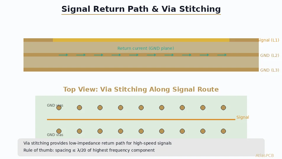
- Return via placement: When signals change layers, place return vias within 1mm
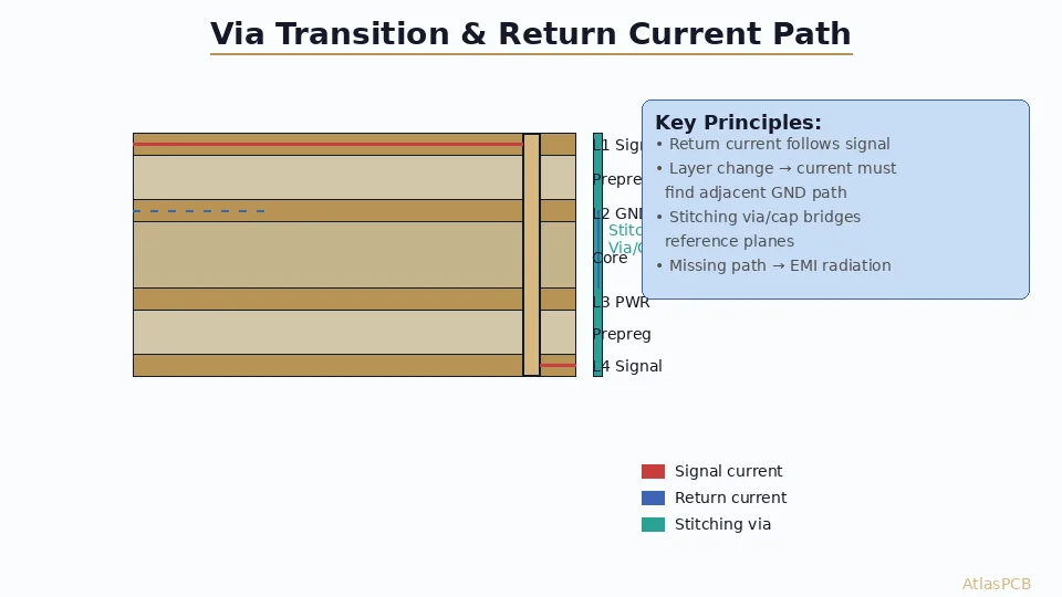
Principle 3: Control Via Transitions
When a signal transitions between layers (via), it changes reference planes. The return current must also transition:
- Same-reference transition: Signal moves between two layers referenced to the same ground plane—no issue
- Different-reference transition: Signal moves from L3 (ref: L2 GND) to L5 (ref: L6 GND)—return current must transfer between planes
Solution: Place a ground stitching via within 1mm of every signal via that changes reference planes. This provides a low-inductance path for return current to follow the signal.
Inductance impact:
- Signal via without nearby ground via: 1-3 nH added inductance
- Signal via with adjacent ground via (<0.5mm): 0.2-0.5 nH added inductance
- Effect on 3.2 Gbps signal: 10-25% eye height degradation without stitching
EMI Reduction Techniques
Board Edge Via Stitching
The PCB edge acts as an antenna aperture. Without containment, edge radiation from the ground-power plane cavity dominates EMI above 1 GHz.
Implementation:
- Place ground vias around the entire board perimeter
- Space vias at ≤λ/20 of highest frequency of concern
- Connect vias to all ground plane layers
- Position within 2mm (50 mil) of board edge
- Size: 0.3mm drill, 0.6mm pad—standard production vias suffice
Spacing calculation:
λ (in FR-4) = c / (f × √εr)
Spacing ≤ λ/20

For 3 GHz: λ = 300/3/√4.2 ≈ 49mm → Spacing ≤ 2.4mm
For 5 GHz: λ = 300/5/√4.2 ≈ 29mm → Spacing ≤ 1.5mm
For 10 GHz: λ = 300/10/√4.2 ≈ 15mm → Spacing ≤ 0.7mm
Via Fencing Around High-Speed Signals
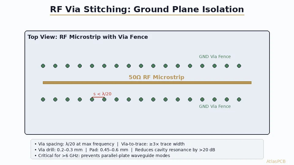
Guard via fences between adjacent high-speed differential pairs reduce crosstalk and contain radiation:
- Place via fence rows parallel to differential pairs
- Spacing: Same λ/20 rule along the fence length
- Fence-to-trace distance: 3× trace width minimum (to avoid impedance impact)
- Connect to adjacent ground planes above and below signal layer
- Particularly important for [DDR5 routing]/blog/pcb-ground-plane-design-emi-ground-bounce-reduction/) and PCIe Gen5+
Slot Antenna Mitigation
When plane splits are unavoidable (different voltage islands, for example):
- Never route high-speed signals across the split
- Bridge the split with decoupling capacitors (0402 size, low ESL) at 5mm intervals
- Minimize slot length: Keep splits as short as possible
- Orient signals parallel to the split (not crossing it)
- Add via stitching along both sides of the split
Cavity Resonance Suppression
The power-ground plane pair forms a parallel-plate resonant cavity. Resonance occurs when board dimensions match λ/2:
For 100×100mm board in FR-4:
- First resonance: ~730 MHz
- Second resonance: ~1.03 GHz (diagonal)
Suppression techniques:
- Distributed decoupling: Capacitors spaced across the board (not just at IC corners)
- Embedded capacitance: Thin dielectric (25-50μm) between power/ground pair
- Resistive termination: Ferrite beads at board edges dissipate resonant energy
- Split via fencing: Ground vias at resonant null points disrupt cavity modes
Ground Bounce: Causes and Solutions
What Causes Ground Bounce?
Ground bounce (simultaneous switching noise, SSN) occurs when multiple output drivers switch simultaneously, creating a transient voltage on the local ground reference:
V_bounce = L_effective × (N × di/dt)Where:
- L_effective = total ground inductance (via + trace + lead)
- N = number of simultaneously switching outputs
- di/dt = rate of current change per output
For a typical DDR5 interface:
- 32 DQ pins switching simultaneously
- Each pin: 10 mA in 100 ps (di/dt = 100 A/μs)
- Package ground inductance: 0.5 nH per pin
- V_bounce = 0.5nH × 32 × 100A/μs = 1.6V (catastrophic without mitigation)
Ground Bounce Mitigation Strategies
1. Minimize ground inductance per pin:
- Multiple ground vias per BGA component (minimum 1:4 ratio GND:signal)
- Wide, short ground traces between BGA pad and via
- Via-in-pad for ground balls (eliminates trace inductance)
- Power/ground plane pair directly beneath BGA layer
2. Distribute switching in time:
- Staggered output enable timing (spread spectrum clocking)
- Avoid simultaneous byte-lane switching in memory interfaces
- Use ODT (On-Die Termination) to reduce switching current amplitude
3. Local charge reservoir:
- Bulk capacitors (10-22μF) within 3mm of power pins
- Decoupling capacitors (100nF) within 1mm of power pins
- Ultra-low inductance capacitors (X2Y, IDC) for high-frequency energy
- [Embedded capacitance planes]/blog/16-layer-pcb-stackup-design-en/) for sub-nanosecond response
4. Power plane design:
- Dedicated power/ground pair with thin dielectric (≤100μm)
- Continuous planes without splits beneath switching outputs
- Return current path analysis ensuring ground current doesn’t flow beneath signal traces
Struggling with EMI or Ground Bounce Issues?
AtlasPCB provides impedance-controlled multilayer stackups with embedded capacitance options and precision ground plane design. Our DFM review catches return path discontinuities before they become compliance failures.
Get Stack-up Quote →Decoupling Capacitor Integration with Ground Planes
Capacitor Placement Strategy
Decoupling capacitors are only effective when their connection inductance to the IC is low enough to supply current at the required speed:
Inductance budget:
- Bulk capacitors (10-100μF): Effective <1 MHz, placement <10mm, via inductance <5 nH acceptable
- Standard decoupling (100nF): Effective 1-100 MHz, placement <3mm, via inductance <1 nH
- High-frequency decoupling (1-10nF): Effective 100 MHz-1 GHz, placement <1mm, via inductance <0.3 nH
- Ultra-high-frequency (10-100pF): Effective 1-10 GHz, embedded or via-in-pad only
Low-Inductance Connection Techniques
Optimized decoupling via pattern:
- Capacitor pad → via → power plane (short path)
- Capacitor pad → via → ground plane (short path)
- Minimize trace length between pad and via (<0.5mm)
- Use multiple vias per pad for high-frequency caps
- Avoid via-to-pad routing through trace—use via-in-pad where possible
Capacitor orientation:
- Mount caps with their longest dimension perpendicular to the IC edge
- Current flow through cap aligned with return path direction
- Avoids magnetic field cancellation that reduces effective capacitance
Embedded Capacitance Technology
Thin-dielectric power/ground plane pairs (25-50μm spacing) provide distributed decoupling:
- Capacitance: ~20 pF/cm² per pair (at 25μm spacing with εr=4)
- Bandwidth: Effective from DC to 5+ GHz (no lead inductance)
- Limitations: Limited total capacitance, expensive dielectric
- Best application: High-frequency bypass for CPU/GPU/FPGA
- Stackup impact: Requires additional layer pair—increases cost by 15-25%
Ground Plane Stackup Strategies
Recommended Stackup Configurations
4-layer (basic high-speed):
L1: Signal + Power pour
L2: Ground plane (SOLID - critical reference)
L3: Power plane (solid, split by voltage)
L4: Signal + Ground pour
6-layer (improved EMI performance):
L1: Signal (referenced to L2)
L2: Ground plane (SOLID)
L3: Signal (referenced to L2 or L4)
L4: Power plane
L5: Signal (referenced to L6)
L6: Ground plane (SOLID)
8-layer (high-speed digital):
L1: Signal/Component (ref: L2)
L2: Ground plane (SOLID)
L3: Signal (ref: L2, L4) — high-speed preferred
L4: Power plane
L5: Ground plane (SOLID)
L6: Signal (ref: L5, L7) — high-speed preferred
L7: Ground plane (SOLID)
L8: Signal/Component (ref: L7)
Key Stackup Rules
- Every signal layer must have an adjacent ground or power reference plane
- Ground planes should bracket the stackup (L2 and second-to-last layer minimum)
- High-speed signals on interior layers (stripline = better shielding than microstrip)
- Thin dielectric (3-5 mil) between signal and reference for tight coupling
- Power-ground pairs with thin dielectric for embedded capacitance
- Symmetric stackup to prevent warpage during lamination
Common Ground Plane Design Mistakes
Mistake 1: Routing Signals on Ground Layers
Problem: Placing a signal trace on a ground plane layer cuts the plane, creating a slot.
Impact: Forces return currents of adjacent signals to detour around the cut, creating crosstalk and radiation.
Fix: Never route on dedicated ground plane layers. If unavoidable, add stitching capacitors bridging the cut at both sides of every crossing trace.
Mistake 2: Insufficient Ground Vias in BGA Fanout
Problem: BGA components have many ground balls, but designers only provide one via per ground ball without considering the current density.
Impact: Ground current crowds into limited vias, creating voltage drops between BGA ground and board ground plane.
Fix: Use via-in-pad for ground balls. For standard fanout, route ground dog-bones as short and wide as possible with immediate via connection. Provide ground via density proportional to signal switching current demand.
Mistake 3: Ignoring Layer Transitions
Problem: Signal vias change reference planes, but no nearby ground via is placed to carry return current between planes.
Impact: Return current travels through displacement current (capacitive coupling between planes)—higher impedance at low frequencies, radiation at high frequencies.
Fix: For every signal via that changes reference plane, place a ground stitching via within 50 mil (1.27mm). For differential pairs, place ground vias on both sides of the pair.
Mistake 4: Thermal Relief on High-Current Ground Pads
Problem: Standard thermal relief (spoke pattern) on ground pads connected to ground planes adds inductance and restricts current flow.
Impact: For decoupling capacitors and IC ground pins, thermal relief adds 0.5-2nH of inductance—defeating the purpose of low-inductance decoupling.
Fix: Use direct connections (no thermal relief) for:
- Decoupling capacitor ground pads
- BGA ground balls (especially on fine-pitch devices)
- Power module ground connections
- Any pad where inductance budget is <1 nH
Use thermal relief only for hand-soldered through-hole connectors and non-critical ground connections.
Mistake 5: Split Ground Under Mixed-Signal IC
Problem: Splitting the ground plane beneath an IC that has both analog and digital ground pins, thinking this “isolates” noise.
Impact: Return currents from digital signals routed over the analog ground (and vice versa) must cross the split—creating exactly the noise coupling you tried to prevent.
Fix: Use a solid ground plane. Partition the LAYOUT (component and trace placement) to separate analog and digital—not the ground plane. Let the IC manufacturer’s reference design guide the specific grounding topology.
Simulation and Verification
Power Integrity Simulation
Tools for ground bounce and plane resonance analysis:
- Ansys SIwave: Full-wave power/ground plane analysis
- Keysight PathWave: Power delivery network optimization
- Cadence Sigrity PowerDC/PowerSI: DC drop + AC impedance analysis
- Altium PDN Analyzer: Integrated power delivery network tool
What to simulate:
- Target impedance vs. frequency (should be flat <target from DC to several GHz)
- Resonant frequencies and their Q-factors
- Current density distribution under transient loads
- Via transition impedance discontinuities
EMI Pre-Compliance Estimation
Before building prototypes, estimate EMI performance:
- Maximum radiated emission from slot antennas (calculate slot resonant frequency)
- Board edge radiation prediction based on via stitching spacing
- Cable radiation coupling through ground plane discontinuities
- Heatsink radiation from connection to board ground
Post-Layout Verification Checklist
- No high-speed signals cross ground plane splits/slots
- All signal layer transitions have adjacent ground stitching vias
- Board edge via stitching complete at ≤2mm spacing
- Decoupling capacitor connections have <1 nH loop inductance
- BGA ground ball via density meets switching current demand
- No routing on dedicated ground plane layers
- Return current path analysis passes for critical nets
- Power/ground plane cavity resonances identified and suppressed
Conclusion: Ground Planes as Active Design Elements
Ground planes are not passive copper fill—they are active electromagnetic structures that determine your product’s EMI performance, signal integrity, and noise margins. Treating ground plane design with the same rigor as signal routing transforms compliance testing from a gamble into a predictable outcome.
Key principles to remember:
- Continuity is king: Solid, unbroken ground planes under all high-speed signals
- Return current requires a path: Every layer transition needs a ground stitching via
- Slots are antennas: Any ground plane discontinuity radiates proportional to its length
- Inductance determines bounce: Minimize ground inductance with multiple short-path vias
- Decoupling loop area matters: Capacitor effectiveness depends on connection geometry, not just capacitance value
Invest time in ground plane design early in the layout process. Fixing EMI failures after fabrication costs 10-100× more than getting the ground architecture right during initial routing.
Designing high-speed digital boards? AtlasPCB fabricates [controlled impedance multilayer PCBs]/blog/controlled-impedance-pcb-stackup-design-rules-en/) with tight dielectric tolerance (±5%) for predictable signal integrity. Our DFM review includes ground plane continuity verification and stackup impedance modeling. Get a quote for your next high-speed design.
About AtlasPCB — We specialize in complex PCB manufacturing for HDI, RF, and high-reliability applications. Explore our impedance-controlled PCB manufacturing . Every order includes free engineering review. Get your quote.
Reviewed by AtlasPCB Engineering Team — IPC-certified manufacturing specialists with 15+ years of production experience in HDI, RF, and high-reliability PCB fabrication. Content based on factory floor data and real customer design reviews.
- ground plane
- EMI
- ground bounce
- signal integrity
- PCB design
- via stitching
- decoupling
- high-speed digital