· AtlasPCB Engineering · Engineering · 11 min read
Any-Layer HDI PCB Design: When to Go Beyond 2+N+2 and How to Optimize for Wearables and SiP Modules
Advanced guide to any-layer HDI PCB design covering when to use ALIS (any-layer interconnect structure) vs standard HDI buildups, microvia stacking strategies, cost drivers, material selection for ultra-thin substrates, and design optimization for wearable electronics and System-in-Package modules.
Introduction: The Routing Density Problem
Modern electronics are shrinking. Wearable devices, hearing aids, AR glasses, medical implants, and IoT sensors demand increasingly complex circuits packed into impossibly small form factors. Simultaneously, semiconductor packages are getting denser—fine-pitch BGAs at 0.3-0.4mm pitch with 500-2000+ pins require enormous routing resources just to fan out signals from beneath the package.
Standard multilayer PCBs hit a wall. Even with [via-in-pad technology]/blog/pcb-via-in-pad-plated-over-design/), mechanical through-vias consume valuable routing space on inner layers. Standard HDI buildups (1+N+1, 2+N+2) help by adding microvia layers, but they still rely on a rigid core with through-vias that limit routing flexibility.
Any-layer HDI—also known as ALIS (Any Layer Interconnect Structure) or ALIVH (Any Layer Inner Via Hole, Panasonic’s branded process)—removes these constraints entirely. By building the entire board from sequential microvia layers with copper-filled stacked vias on every layer, any-layer HDI gives designers the ultimate routing freedom: any pad on any layer can connect to any other pad on any other layer.
This guide covers when any-layer HDI is genuinely necessary (vs. expensive overkill), how to design for it, and the manufacturing realities that affect cost and reliability. For foundational HDI concepts, see our [HDI PCB stackup design guide]/blog/hdi-pcb-stackup-design-advanced/) and [microvia stacking reliability analysis]/blog/hdi-microvia-stacked-vs-staggered-reliability/).
Understanding HDI Buildup Hierarchy
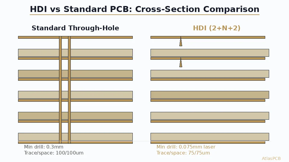
Standard Multilayer (No HDI)
- Through-vias only (mechanically drilled, minimum 0.2mm)
- All vias span the entire board thickness
- Minimum via pitch: ~0.6mm (0.3mm drill + 0.3mm annular ring clearance)
- Typical for: general electronics, consumer products, simple power electronics
Type I HDI: 1+N+1
- One microvia layer on each side of a core
- Microvias connect layer 1↔2 and layer (N-1)↔N only
- Core still has mechanical through-vias
- Typical for: smartphones (basic), networking equipment, automotive ECUs
Type II HDI: 2+N+2
- Two microvia layers on each side
- Microvias can be stacked (layer 1→2→3) or staggered
- Core through-vias still present
- Typical for: high-end smartphones, tablets, compact servers
Type III HDI: Any-Layer (ALIS)
- No conventional core—all layers are buildup layers
- Stacked copper-filled microvias connect any layer to any other layer
- No mechanical through-vias anywhere in the stackup
- Typical for: wearables, hearing aids, SiP modules, medical implants, Apple Watch-class products
Visual Comparison
Standard Multilayer          1+N+1 HDI              Any-Layer HDI
┌─────────────────┐   ┌─────────────────┐   ┌─────────────────┐
│ L1 ═══╤═══╤════ │   │ L1 ●──╤════╤═══ │   │ L1 ●━━●━━●━━●━ │
│       │   │     │   │    │  │    │    │   │    ┃  ┃  ┃  ┃  │
│ L2 ───┤   │──── │   │ L2 ●──┤    │─── │   │ L2 ●━━●━━●━━●━ │
│       │   │     │   │       │    │    │   │    ┃  ┃  ┃  ┃  │
│ L3 ───┤   │──── │   │ L3 ───┤    │─── │   │ L3 ●━━●━━●━━●━ │
│       │   │     │   │       │    │    │   │    ┃  ┃  ┃  ┃  │
│ L4 ───┤   │──── │   │ L4 ───┤    │─── │   │ L4 ●━━●━━●━━●━ │
│       │   │     │   │       │    │    │   │    ┃  ┃  ┃  ┃  │
│ L5 ───┤   ├──── │   │ L5 ●──┤    │─── │   │ L5 ●━━●━━●━━●━ │
│       │   │     │   │    │  │    │    │   │    ┃  ┃  ┃  ┃  │
│ L6 ═══╧═══╧════ │   │ L6 ●──╧════╧═══ │   │ L6 ●━━●━━●━━●━ │
└─────────────────┘   └─────────────────┘   └─────────────────┘
  ═ through-via          ● microvia           ● stacked microvia
                         ═ through-via         (copper-filled)
When Any-Layer HDI Is Justified
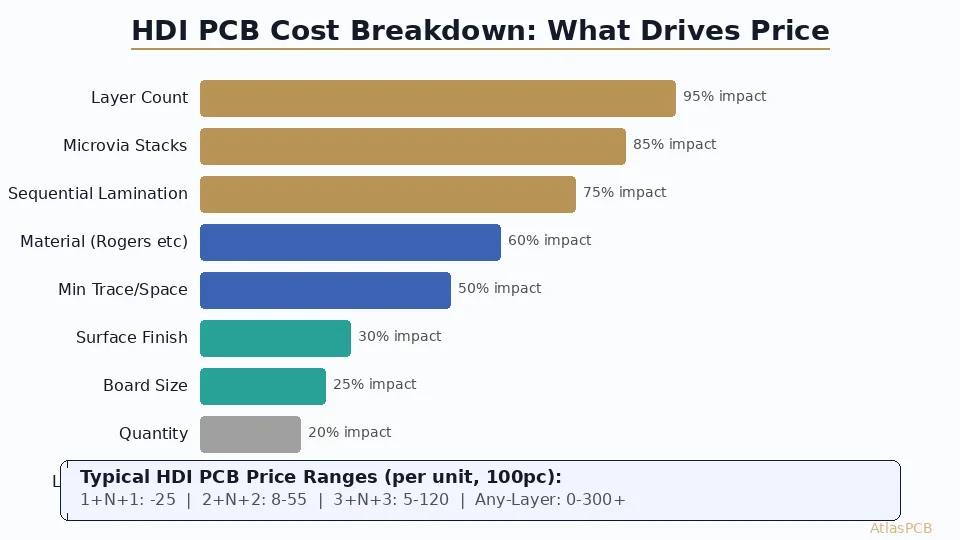
Any-layer HDI costs 3-5× more than standard HDI and 8-15× more than standard multilayer. Use it only when genuinely necessary:
Decision Criteria
✅ Use Any-Layer When:
- BGA pitch ≤ 0.35mm with full fan-out required
- Board thickness < 0.5mm with 6+ signal layers needed
- Component density requires routing on all layers with no room for through-via keepouts
- SiP (System-in-Package) module substrate design
- Medical implantables where size and reliability are paramount
- High-frequency applications where via stubs from through-vias degrade signal integrity (though [back-drilling]/blog/pcb-backplane-design-high-speed/) is the cheaper alternative for this)
❌ Don’t Use Any-Layer When:
- 2+N+2 HDI can achieve adequate routing density (check first!)
- Board thickness is not constrained below 0.8mm
- Budget is a primary concern (prototype quantities are especially expensive)
- Design can be achieved with via-in-pad on standard multilayer
Cost Comparison (8-Layer Board, 100 pcs)
| Technology | Approximate Cost/Board | Board Thickness |
|---|---|---|
| Standard multilayer | $15-25 | 1.2-1.6mm |
| 1+N+1 HDI | $30-50 | 0.8-1.2mm |
| 2+N+2 HDI | $50-90 | 0.6-1.0mm |
| Any-layer HDI | $120-250 | 0.3-0.6mm |
Prices are indicative for 50×50mm board, 100-piece production run
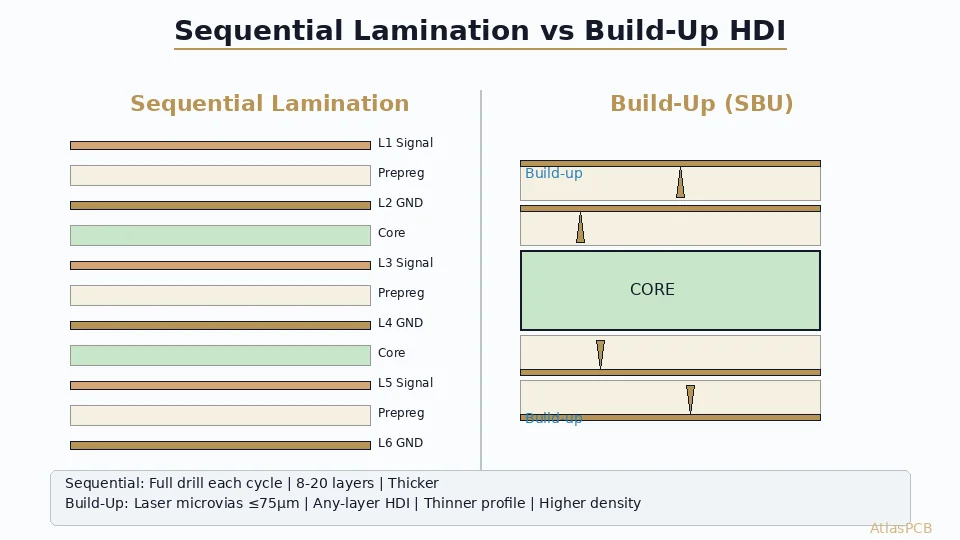
Any-Layer Stackup Design
Layer Stack Principles
In any-layer HDI, the stackup is built from repeated buildup sequences. There’s no traditional core laminate. Instead:
- Start with a thin carrier or temporary core
- Build up layers sequentially with laser-drilled, copper-filled microvias
- Each dielectric layer is typically 25-60μm of resin-coated copper foil (RCC) or ABF-type buildup film
- Copper thickness is typically 12-18μm per layer (thinner than standard PCB copper)
Example: 8-Layer Any-Layer for Wearable
Layer 1 (Top):    Signal/Component — 12μm Cu
  Dielectric:     40μm ABF buildup
Layer 2:          Ground plane — 12μm Cu
  Dielectric:     40μm ABF buildup
Layer 3:          Signal routing — 12μm Cu
  Dielectric:     40μm ABF buildup
Layer 4:          Power plane — 12μm Cu
  === Symmetry axis ===
Layer 5:          Power plane — 12μm Cu
  Dielectric:     40μm ABF buildup
Layer 6:          Signal routing — 12μm Cu
  Dielectric:     40μm ABF buildup
Layer 7:          Ground plane — 12μm Cu
  Dielectric:     40μm ABF buildup
Layer 8 (Bottom): Signal/Component — 12μm Cu

Total thickness: ~0.42mm (without solder mask)
Microvia Specifications
| Parameter | Standard Any-Layer | Advanced Any-Layer |
|---|---|---|
| Via drill diameter | 75-100 μm | 50-75 μm |
| Via capture pad | 150-200 μm | 100-150 μm |
| Via pitch (center-to-center) | 300-400 μm | 200-300 μm |
| Maximum stack depth | 4-6 layers | 6-8 layers |
| Fill method | Copper electrofill | Copper electrofill |
| Fill quality | ≤25μm dimple | ≤15μm dimple |
| Aspect ratio (depth:diameter) | 0.8:1 typical | Up to 1:1 |
Via Stacking Reliability
Stacked microvias in any-layer HDI must be copper-filled (not conformal plated or paste-filled). The copper fill provides:
- Structural integrity across thermal cycling
- Low resistance electrical connection
- Flat landing pad for the next via in the stack
For stacks deeper than 4 layers, reliability becomes a concern. See our detailed analysis of [stacked vs staggered microvia reliability]/blog/hdi-microvia-stacked-vs-staggered-reliability/). Key takeaway: stacks of 3-4 are highly reliable with proper copper fill. Stacks of 5-6 require IST (Interconnect Stress Testing) validation. Stacks of 7+ are pushing manufacturing limits and should be avoided in designs requiring IPC Class 3 reliability.
Designing a Compact HDI Board?
AtlasPCB manufactures any-layer HDI PCBs with microvia stacks up to 6 layers deep. Our engineering team helps optimize your stackup for cost, thickness, and reliability.
Get an HDI Stackup Review →Design Optimization for Wearable Electronics
The Wearable Challenge
Wearable electronics impose simultaneous constraints that push toward any-layer HDI:
- Thickness: Total PCB+components < 1.0mm (PCB alone often < 0.5mm)
- Area: Board dimensions driven by product form factor, not circuit complexity
- Component density: BLE SoC, IMU, PMIC, flash, sensor ICs on both sides of a coin-sized board
- Reliability: Must survive thousands of flex cycles from body movement (not flex PCB territory, but mild flex)
- Battery life: Compact power delivery network with low impedance
Design Strategies for Wearables
1. Use both sides for components Any-layer HDI enables true double-sided assembly with equal routing access to both sides. Place the main SoC on one side and supporting ICs on the other. Stacked microvias provide direct vertical connections between top and bottom BGA arrays.
2. Minimize layer count Even though any-layer HDI can scale to many layers, every layer adds cost and thickness. For most wearables, 6-8 layers is sufficient:
- 2 signal layers (top + bottom component layers)
- 2 ground planes (essential for EMI and signal integrity—see our [EMC design guide]/blog/emc-emi-pcb-design/))
- 2 power planes or mixed power/signal layers
3. Aggressive trace/space Any-layer HDI fabricators typically support 50/50μm trace/space as standard, with 35/35μm available using mSAP (modified Semi-Additive Process). This is 2-3× denser than standard PCB routing, enabling escape routing from 0.35mm pitch BGAs without excessive layer count.
4. Embedded passives For the ultimate in space savings, consider [embedded components]/blog/embedded-component-pcb-technology/)—resistors and capacitors formed within the PCB layers. This eliminates surface-mount footprints and improves electrical performance (shorter connections, lower parasitic inductance).
Wearable Case Study: Smartwatch Main Board
Requirements: 8-layer, 0.4mm thick, 25×30mm, 0.4mm pitch BGA SoC with 289 balls, BLE, IMU, PMIC, 4GB flash
Stackup solution:
L1: Components + signal routing (12μm Cu, 50/50μm trace/space)
D1: 35μm ABF
L2: Ground (continuous, stitched to all edges)
D2: 40μm ABF
L3: Signal + power routing
D3: 35μm ABF
L4: Power planes (segmented for 1.8V, 3.3V, VBAT)
D4: 35μm ABF
L5: Power planes (continued)
D5: 40μm ABF
L6: Signal routing
D6: 35μm ABF
L7: Ground (continuous)
D7: 35μm ABF
L8: Components + signal routing
Total: ~0.41mm
Design Optimization for SiP Modules
System-in-Package Overview
SiP modules package multiple bare dies, passives, and sometimes MEMS sensors onto a single PCB substrate, which is then overmolded and treated as a single component. Examples include Apple’s S-series (Watch), Qualcomm’s QCS modules, and Nordic’s SiP variants.
Any-layer HDI is the standard substrate technology for SiP modules because:
- Wire bond and flip-chip compatibility: Fine-pitch landing pads for both assembly methods
- Impedance control: Controlled impedance traces between dies for high-speed interconnect
- Thermal management: Thermal vias from die attach pads to bottom-side thermal pad
- Testability: Test pads accessible on the substrate before overmolding
SiP Substrate Design Rules
| Parameter | Typical Range | Notes |
|---|---|---|
| Trace width/space | 30-50 μm | mSAP process required below 40μm |
| Via drill | 50-75 μm | Laser drilled |
| Via pad | 100-150 μm | Copper filled |
| Wire bond pad size | 80-120 μm | Gold or copper wire |
| Flip-chip pad pitch | 100-200 μm | Solder-capped or Cu pillar |
| Substrate thickness | 0.2-0.4 mm | 4-8 layers typical |
| Dielectric thickness | 20-35 μm | Ultra-thin ABF or BT resin |
Differences from Standard PCB Design
Designing SiP substrates requires a different mindset than standard PCB design:
- Units are in micrometers, not millimeters
- Panelization uses strip format (similar to IC substrate manufacturing) rather than standard PCB panels
- Surface finish is typically ENEPIG for wire bond compatibility—see our [ENEPIG guide]/blog/enepig-vs-enig-surface-finish-wire-bonding/)
- Overmold interaction: The substrate must withstand the thermal and mechanical stress of epoxy molding compound (EMC) application at 175°C
- Known-good-die (KGD) testing: Die quality must be verified before attachment, because rework after assembly is essentially impossible
Material Selection for Any-Layer HDI
Dielectric Materials
| Material | Dk @ 1GHz | Df @ 1GHz | Tg (°C) | Typical Use |
|---|---|---|---|---|
| ABF GX-92 | 3.3 | 0.008 | 218 | IC substrates, SiP |
| ABF GY-11 | 3.3 | 0.006 | 213 | High-frequency SiP |
| BT resin | 3.8 | 0.012 | 220 | Standard HDI, module substrates |
| Low-Dk RCC | 3.4 | 0.008 | 175 | Cost-optimized any-layer |
| Megtron 4 (thin) | 3.4 | 0.005 | 210 | High-speed any-layer |
For wearable applications where RF performance matters (BLE, Wi-Fi, GPS antennas), choose low-Dk/low-Df dielectrics. For more on high-frequency material selection, see our [RF material comparison guide]/blog/high-frequency-pcb-substrate-selection-dk-df/).
Copper Foil
Any-layer HDI typically uses 12μm copper foil (vs. 17-35μm for standard PCBs). Ultra-thin 9μm copper is available for the finest trace widths (< 40μm) but requires careful handling during lamination.
For mSAP processing: start with 3-5μm flash copper, then plate up to target thickness. This produces the finest lines but requires specialized chemistry and tight process control.
Reliability Considerations
Thermal Cycling Performance
Any-layer HDI boards with properly copper-filled stacked microvias typically pass 1000 cycles of -40°C to +125°C thermal cycling per IPC-TM-650 standards. Critical factors:
- Copper fill quality: Voids in via fill are the primary failure mechanism. Specify ≤25% void area per IPC-6012 Class 3
- CTE matching: Ultra-thin dielectrics with high filler content help match CTE between copper and dielectric
- Stack depth: Limit stacks to 4 layers for Class 3 reliability. Use microsection verification on production panels
IST (Interconnect Stress Test)
For high-reliability applications (medical, aerospace), specify IST testing on production panels. IST applies accelerated thermal cycling by resistive heating of the test coupon, detecting resistance changes that indicate microvia degradation. A pass threshold of < 10% resistance increase after 500 IST cycles is standard.
Moisture Sensitivity
Ultra-thin any-layer boards are more susceptible to moisture absorption than standard FR-4 boards. Specify JEDEC Level 3 or better moisture sensitivity handling. Bake boards at 125°C for 4-8 hours before assembly if storage time exceeds 168 hours from unsealing. See our [moisture sensitivity guide]/blog/pcb-moisture-sensitivity-baking/) for detailed procedures.
DFM Rules Summary
| Rule | Any-Layer Requirement |
|---|---|
| Minimum trace width | 50μm standard, 35μm with mSAP |
| Minimum trace space | 50μm standard, 35μm with mSAP |
| Microvia drill diameter | 75μm (standard), 50μm (advanced) |
| Via pad diameter | 2× drill + 50μm minimum |
| Maximum via stack | 4-6 layers (discuss with fabricator) |
| Board thickness | 0.2-0.6mm typical for any-layer |
| Registration tolerance | ±25μm layer-to-layer |
| Solder mask registration | ±30μm |
| Minimum solder mask dam | 50μm (40μm with LDI) |
Conclusion: The Any-Layer Decision Framework
Before committing to any-layer HDI:
- Exhaust standard options first: Can 2+N+2 HDI meet your routing needs? Use your EDA tool’s auto-router or fanout analysis to check
- Quantify the constraint: Is it BGA pitch, board thickness, routing density, or signal integrity driving the need?
- Budget accordingly: Any-layer prototypes cost $200-500+ per board at small quantities. Plan for 3-4× NRE compared to standard HDI
- Choose your fabricator carefully: Not all HDI fabricators have any-layer capability. Verify their process qualifications, especially copper fill quality and maximum stack depth
- Design for test: Include IST coupons and cross-section locations on your panel for production verification
Working on a compact HDI design? AtlasPCB’s HDI manufacturing facility handles any-layer builds up to 16 layers with copper-filled stacked microvias. Our engineering team provides stackup consultation and DFM review to optimize your design for manufacturability and cost. Submit your design for expert review →
Further Reading
- [HDI PCB Design for 5G Antenna Integration: Signal Integrity Challenges in Millimeter-Wave Applications]/blog/hdi-5g-antenna-integration-pcb-design/)
- [Via-in-Pad Design: Filled, Capped, and Plated Over — Complete Guide]/blog/via-in-pad-design/)
- [PCB Copper Plating Process: Electroless vs Electrolytic Copper for HDI Vias and High-Density Interconnects]/blog/pcb-copper-plating-electroless-vs-electrolytic-hdi-vias/)
- [PCB Via Reliability Testing: IST, Thermal Cycling, and IPC-6012 Compliance for Microvias]/blog/pcb-via-reliability-testing/)
- [Buried Via Technology in High-Density PCBs: Design Rules, Fabrication & Cost]/blog/pcb-buried-via-technology/)
- HDI PCB Manufacturing
About AtlasPCB — We specialize in complex PCB manufacturing for HDI, RF, and high-reliability applications. Explore our HDI PCB manufacturing capabilities, or get an multilayer PCB fabrication up to 30 layers . Every order includes free engineering review. Get your quote.
Reviewed by AtlasPCB Engineering Team — IPC-certified manufacturing specialists with 15+ years of production experience in HDI, RF, and high-reliability PCB fabrication. Content based on factory floor data and real customer design reviews.
- HDI PCB
- any-layer
- ALIS
- microvia
- SiP
- wearable electronics
- fine-pitch BGA
- PCB stackup
- via-in-pad
- advanced manufacturing