· AtlasPCB Engineering · Engineering · 11 min read
Laser Direct Imaging (LDI) in PCB Manufacturing: Accuracy, Benefits & When to Specify
Understand how Laser Direct Imaging (LDI) improves PCB accuracy over conventional photolithography. Learn LDI capabilities, fine-line requirements, and when to specify LDI for your design.
Introduction: From Film to Laser
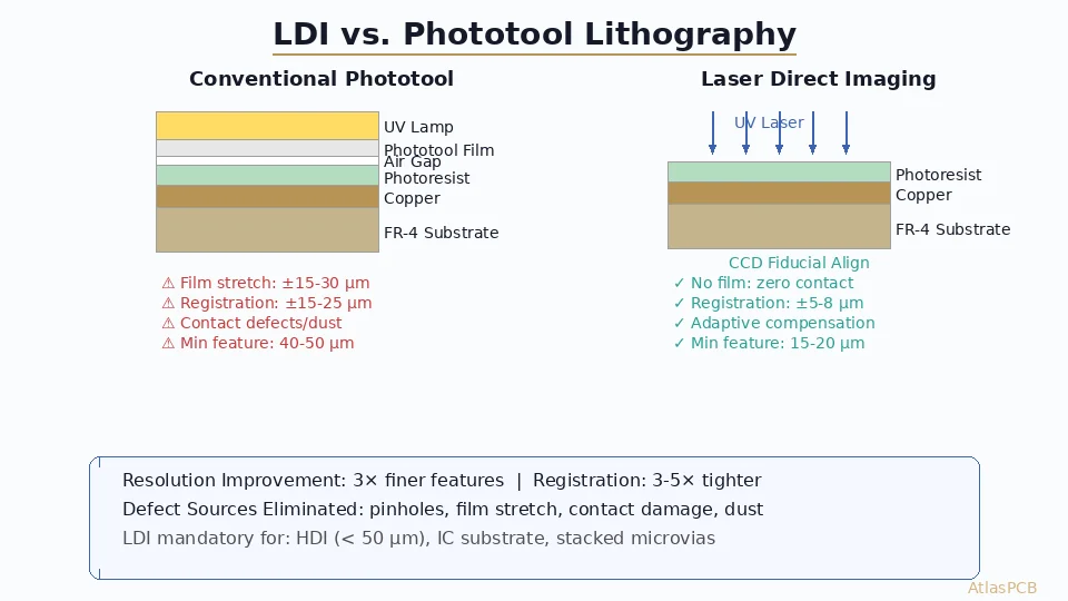
For decades, PCB circuit patterns were transferred from design data to copper through a chain of physical media: Gerber data → photoplotted film → contact exposure onto photoresist → develop → etch. Each step introduced variability. Film stretched with humidity, contact frames had uneven pressure, and registration between film and panel depended on pin alignment that degraded with use.
Laser Direct Imaging (LDI) eliminates the weakest links in this chain by removing film entirely. Instead of projecting light through a physical film, an LDI system uses precisely controlled UV lasers to write the circuit pattern directly onto the photoresist-coated panel. The result is a fundamental improvement in accuracy, repeatability, and process control.
Today, LDI has transitioned from a premium technology reserved for the most demanding designs to a mainstream production tool adopted by fabricators worldwide. Understanding when to specify LDI — and what it can and cannot do — is essential knowledge for PCB designers working on fine-pitch, high-density, or controlled-impedance circuits.
How LDI Works
System Architecture
An LDI system consists of several key components:
UV laser source: Typically a 355 nm or 375 nm wavelength laser, sometimes multiple lasers for throughput. Advanced systems use 405 nm LED sources with DMD (Digital Micromirror Device) technology.
Beam delivery optics: Galvanometer mirrors or polygon scanners that direct the laser beam across the panel surface with sub-micron positioning accuracy.
Panel alignment system: Cameras that locate fiducial marks (registration targets) on each panel and calculate the scaling, rotation, and offset corrections needed to align the image data to the actual panel dimensions.
Motion system: A precision stage that positions the panel under the imaging head. Some systems move the panel; others move the imaging head; advanced systems use a combination.
Software: Converts Gerber/ODB++ data into rasterized imaging data and applies the real-time scaling corrections calculated from the alignment measurement.
Imaging Process
The LDI imaging process follows these steps:
- Panel loading: The photoresist-coated panel is loaded onto the LDI stage
- Alignment measurement: Cameras locate fiducial marks on the panel and measure actual panel dimensions
- Scaling correction: Software calculates the difference between nominal and actual panel dimensions and adjusts the image data accordingly (typically ±50-200 ppm)
- Exposure: The laser writes the circuit pattern onto the photoresist, line by line, at speeds of 5-50 mm²/ms depending on the system
- Unloading: The exposed panel moves to the develop process
Total imaging time per panel side: 30-90 seconds for standard designs, up to 2-3 minutes for extremely dense designs.
LDI vs. Conventional Contact Exposure
| Parameter | Conventional (Film) | LDI |
|---|---|---|
| Registration accuracy | ±25-50 µm | ±10-15 µm |
| Minimum trace/space | 75-100 µm (3-4 mil) | 50-75 µm (2-3 mil) production |
| Film cost | $50-200/layer/design | None |
| Panel scaling compensation | None (fixed film) | Real-time per panel |
| Exposure time per side | 3-8 seconds | 30-90 seconds |
| Repeatability | Film-dependent | Excellent (digital) |
| Environmental sensitivity | Film stretches with humidity | None |
| Setup time for new design | Film generation (hours-days) | Data loading (minutes) |
| Defect sources | Film scratches, dust, pinholes | Resist defects only |
Key Advantages of LDI
1. Superior Registration Accuracy
The most impactful advantage of LDI is its ability to measure and compensate for individual panel dimensional variations. Every panel that enters the LDI system is measured, and the image is scaled to match the actual panel dimensions.
This matters because:
- Lamination causes non-uniform scaling: During lamination, panels expand and contract unevenly due to copper distribution, prepreg flow, and press temperature gradients. A typical panel may have ±100-200 ppm dimensional variation from nominal.
- Film cannot compensate: A fixed film has one set of dimensions that must match all panels. Panels that have expanded or contracted differently will have misregistration.
- LDI adapts to each panel: By measuring each panel and adjusting the image, LDI eliminates the systematic component of registration error.
For designs with tight annular ring requirements — such as [HDI with microvias]/blog/hdi-pcb-design-guide/) or dense BGA patterns — this per-panel compensation is the difference between 95% yield and 99.5% yield.
2. Fine-Line Capability
LDI enables production of finer traces and spaces than conventional contact exposure:
| Feature | Conventional Production | LDI Production | LDI Advanced |
|---|---|---|---|
| Trace width | ≥75 µm (3 mil) | ≥50 µm (2 mil) | ≥25 µm (1 mil) |
| Space width | ≥75 µm (3 mil) | ≥50 µm (2 mil) | ≥37.5 µm (1.5 mil) |
| Annular ring | ≥75 µm (3 mil) | ≥50 µm (2 mil) | ≥25 µm (1 mil) |
| Pad resolution | ≥125 µm (5 mil) | ≥75 µm (3 mil) | ≥50 µm (2 mil) |
Fine-line capability depends on more than just the imaging system — photoresist type, copper thickness, etch process, and cleanliness all play roles. But the imaging system sets the ceiling: you cannot achieve 50 µm traces if the imaging system cannot resolve them.
3. Elimination of Film-Related Defects
Phototools (films) are a significant source of defects in conventional processing:
- Pinholes: Dust particles on film create unwanted openings, especially problematic for solder mask
- Scratches: Film handling creates linear defects that can bridge traces or open gaps
- Dimensional instability: Film expands ~20 ppm/°C and ~10 ppm/%RH, causing dimensional drift between exposures
- Wear: Contact exposure physically presses the film against the panel; after hundreds of exposures, the film degrades
LDI eliminates all film-related defects. The only defect sources remaining are in the photoresist itself (coating defects, particles on the panel) and the LDI system optics (which are enclosed and clean-room maintained).
4. Rapid Design Changes
In a conventional process, changing a design requires generating new film — a process that takes hours to days depending on the phototool facility. With LDI, design changes are implemented by loading new data files, which takes minutes.
This advantage is particularly valuable for:
- Quick-turn prototyping: No waiting for film generation
- Engineering changes during production: Can implement ECOs immediately
- Multi-part panelization: Different designs on the same panel without multiple film sets
5. Controlled Impedance Improvement
For [controlled impedance PCBs]/blog/controlled-impedance-pcb/), LDI provides two significant benefits:
Trace width accuracy: LDI trace width variation is typically ±5-8 µm compared to ±10-15 µm for conventional exposure. For a 100 µm trace where impedance depends on width, this reduces impedance variation by approximately 50%.
Panel-to-panel consistency: Because LDI compensates for panel scaling, the dielectric thickness (which also affects impedance) is better matched to the trace width, since both are referenced to the same panel dimensions.
These improvements make ±5% impedance tolerance achievable in production, compared to ±10% with conventional processes.
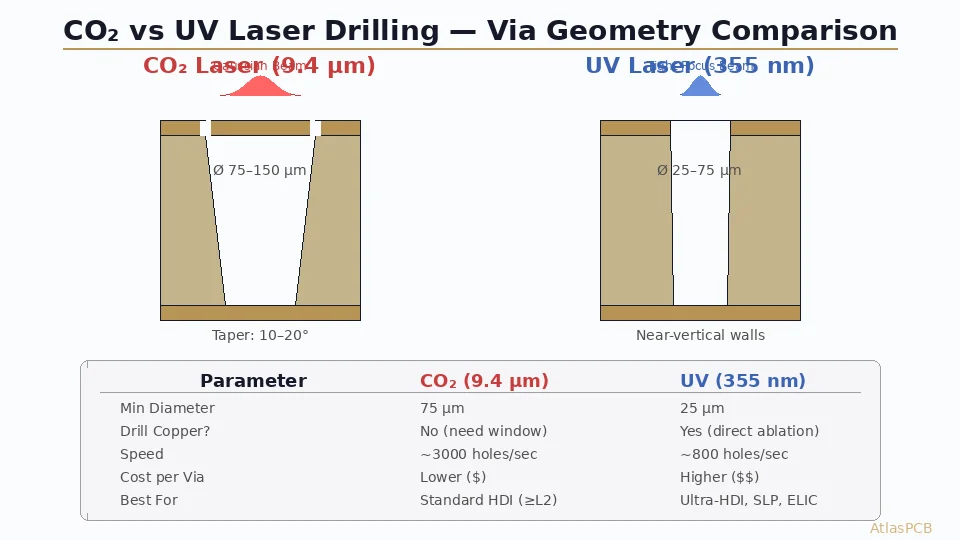
LDI Technology Types
Laser-Based LDI (Scanning)
The original LDI technology uses one or more focused laser beams that scan across the panel:
- Wavelength: 355 nm (UV) or 375 nm (near-UV)
- Spot size: 10-25 µm
- Speed: Moderate (40-90 seconds per side for 18×24” panel)
- Resolution: Excellent (≤25 µm features achievable)
- Best for: Fine-line applications, advanced HDI
DMD-Based LDI (Projection)
Digital Micromirror Device (DMD) systems use an array of microscopic mirrors to project a full image area simultaneously:
- Light source: 365-405 nm LED or laser array
- Pixel size: 10-25 µm per mirror
- Speed: Fast (20-60 seconds per side)
- Resolution: Very good (≤50 µm features standard)
- Best for: High-volume production with good resolution
Comparison for Design Selection
| Criterion | Laser Scanning | DMD Projection |
|---|---|---|
| Best resolution | ≤25 µm | ≤50 µm |
| Speed | Moderate | Fast |
| Capital cost | Higher | Moderate |
| Operating cost | Low | Low |
| Solder mask imaging | Good | Excellent |
| Inner layer imaging | Excellent | Very Good |
Most modern fabricators have standardized on DMD-based LDI for general production and laser-scanning LDI for the most demanding fine-line work.
When to Specify LDI
Design Triggers for LDI
Specify LDI in your fabrication notes when your design includes any of the following:
- Fine lines: Trace/space ≤100 µm (4 mil) on any layer
- Dense BGAs: 0.4 mm pitch or finer, or ≥0.65 mm pitch with via-in-pad
- Tight annular ring: <75 µm (3 mil) on any via
- Controlled impedance ±5%: Requires the trace width accuracy only LDI provides
- HDI features: [Microvias]/blog/hdi-pcb-design-guide/), stacked vias, any-layer structures
- Solder mask registration: Solder mask dam <75 µm (3 mil) between pads
- High layer count: >12 layers where cumulative registration error matters
- Flex and rigid-flex: Where dimensional instability during processing is highest
How to Specify LDI
In your fabrication drawing or notes, include:
IMAGING: Laser Direct Imaging (LDI) required for all layers
         (or specify: "LDI required for inner layers L3-L6 only")
If your design has fine-line features on specific layers only, you can specify LDI selectively to potentially reduce cost:
IMAGING: LDI required for L3, L4 (fine-line layers, 3/3 mil trace/space)
         Conventional exposure acceptable for L1, L2, L5, L6
When LDI Is Not Necessary
LDI adds no meaningful benefit for:
- Designs with ≥150 µm (6 mil) trace/space on all layers
- Simple 1-2 layer boards with loose tolerances
- Large-feature power electronics with >200 µm features
- Prototypes where slight registration variation is acceptable
However, many fabricators have fully transitioned to LDI for all production, making it the default process regardless of design complexity. In these cases, there is no cost premium for LDI — you get it automatically.
LDI and Solder Mask
LDI is equally valuable for solder mask imaging, where registration and resolution directly affect assembly quality:
Solder Mask LDI Benefits
- Dam resolution: LDI achieves solder mask dams down to 50 µm (2 mil) compared to 75-100 µm (3-4 mil) for conventional
- Registration to copper: ±15-25 µm compared to ±50-75 µm for film-based mask exposure
- No film contact damage: Wet solder mask is soft and sticky; film contact can cause defects and sticking
Fine-Pitch Component Implications
For 0.4 mm pitch BGAs and 0201/01005 component pads, solder mask registration is critical:
| BGA Pitch | Pad Size | Gap Between Pads | Solder Mask Dam Required |
|---|---|---|---|
| 0.8 mm | 0.40 mm | 0.40 mm | 0.30 mm — conventional OK |
| 0.65 mm | 0.30 mm | 0.35 mm | 0.25 mm — LDI recommended |
| 0.5 mm | 0.25 mm | 0.25 mm | 0.15 mm — LDI required |
| 0.4 mm | 0.20 mm | 0.20 mm | 0.10 mm — LDI essential, NSMD |
At 0.5 mm pitch and below, solder mask LDI is practically mandatory for reliable assembly.
Impact on DFM and Design Rules
Relaxed vs. Tightened Rules with LDI
LDI enables tighter design rules, but designers must still account for etch, plating, and other process variations:
| Parameter | Without LDI | With LDI | Notes |
|---|---|---|---|
| Min trace width (outer) | 100 µm (4 mil) | 75 µm (3 mil) | Etch undercut is still the limiter |
| Min space (outer) | 100 µm (4 mil) | 75 µm (3 mil) | Copper thickness dependent |
| Min trace width (inner) | 75 µm (3 mil) | 50 µm (2 mil) | Inner layers have thinner copper |
| Min space (inner) | 75 µm (3 mil) | 50 µm (2 mil) | Better etch control on thin copper |
| Annular ring (outer) | 100 µm (4 mil) | 75 µm (3 mil) | Registration is the limiter |
| Annular ring (inner) | 75 µm (3 mil) | 50 µm (2 mil) | Better sub-panel registration |
Important: LDI improves the imaging step, but the total feature accuracy depends on the entire process chain. Always verify capabilities with your fabricator for your specific design requirements.
For a comprehensive view of manufacturability constraints, review our [DFM checklist]/blog/pcb-dfm-checklist/).
LDI in the Context of PCB Manufacturing Evolution
Historical Progression
| Era | Technology | Feature Capability | Registration |
|---|---|---|---|
| 1980s | Diazo film, contact exposure | 200 µm (8 mil) | ±75-100 µm |
| 1990s | Silver halide film, contact exposure | 100 µm (4 mil) | ±50-75 µm |
| 2000s | High-resolution film, vacuum contact | 75 µm (3 mil) | ±25-50 µm |
| 2010s | First-generation LDI | 50 µm (2 mil) | ±15-25 µm |
| 2020s | Advanced LDI (DMD + laser hybrid) | 25 µm (1 mil) | ±10-15 µm |
Future Trends
- EUV and deep-UV LDI: Shorter wavelengths will enable <10 µm features for substrate-like PCBs
- AI-assisted exposure optimization: Machine learning adjusting exposure parameters in real-time based on resist and panel properties
- Integration with AOI: Closed-loop systems where automated optical inspection feeds back to LDI for process correction
- Panel-level packaging: As semiconductor packaging moves to larger panel formats, LDI is the primary imaging technology due to its filmless, scalable nature
Practical Recommendations for Designers
For Standard Designs (≥100 µm Features)
LDI provides a quality improvement but is not strictly necessary:
- Accept the fabricator’s standard process (many already use LDI by default)
- Focus your attention on other yield-critical parameters
- Do not add cost by specifying LDI if your fabricator offers it as standard
For Fine-Line Designs (50-100 µm Features)
LDI is strongly recommended:
- Specify LDI in fabrication notes for all fine-line layers
- Design with LDI-capable rules but maintain ≥10 µm margin above absolute minimums
- Use [via-in-pad]/blog/via-in-pad-design/) with confidence, as LDI provides the registration needed for tight annular rings
- Expect 5-10% cost premium if your fabricator charges separately for LDI
For Advanced HDI Designs (<50 µm Features)
LDI is mandatory:
- Work closely with your fabricator to confirm specific capabilities
- Use modified semi-additive process (mSAP) or additive processes alongside LDI for the finest features
- Specify LDI for both circuit imaging and solder mask
- Request sample production and microsection analysis before committing to volume
Conclusion
Laser Direct Imaging has fundamentally changed what is achievable in PCB manufacturing. By eliminating film and adding per-panel dimensional compensation, LDI delivers the registration accuracy and fine-line capability that modern electronic designs demand. Whether you are designing a 4-layer IoT module with 0.4 mm pitch BGAs or a 20-layer high-speed backplane with controlled impedance, understanding LDI capabilities helps you design confidently within achievable manufacturing limits.
The key takeaway for designers: specify LDI when your design pushes below 100 µm features or requires tight registration. For everything else, you likely already benefit from LDI without knowing it, as the technology has become the standard imaging method at leading fabricators worldwide.
At Atlas PCB, our production lines use state-of-the-art LDI systems for both circuit pattern and solder mask imaging, ensuring the tightest registration and finest features available in the industry. Our engineering team can advise you on the optimal design rules for LDI-based fabrication.
Atlas PCB specializes in fine-line PCB manufacturing with advanced LDI imaging for trace/space down to 50 µm. Contact us for engineering support and a free DFM review on your next project.
Further Reading
- [Rogers PCB Fabrication: Material Sourcing, Lead Times & Quality Control]/blog/rogers-pcb-fabrication/)
- [PCB Manufacturer with Engineering Review: Why Human DFM Audit Matters]/blog/pcb-manufacturer-engineering-review/)
- [ENEPIG vs ENIG: Which PCB Surface Finish for Your Design?]/blog/enepig-vs-enig/)
- [PCB Surface Finish Selection — ENIG vs HASL vs OSP vs Hard Gold vs ENEPIG]/blog/pcb-surface-finish-enig-hasl-osp-hard-gold-enepig/)
- [Medical PCB Manufacturing: FDA Compliance, Traceability & Reliability]/blog/medical-pcb-manufacturing-requirements/)
- Our Manufacturing Capabilities
About AtlasPCB — We specialize in complex PCB manufacturing for HDI, RF, and high-reliability applications. Explore our full PCB manufacturing capabilities, or get an instant online quote . Every order includes free engineering review. Get your quote.
Reviewed by AtlasPCB Engineering Team — IPC-certified manufacturing specialists with 15+ years of production experience in HDI, RF, and high-reliability PCB fabrication. Content based on factory floor data and real customer design reviews.
- ldi
- laser-imaging
- fine-line
- manufacturing