· AtlasPCB Engineering · Engineering · 6 min read
PCB Creepage and Clearance: IPC-2221B High-Voltage Spacing Design Guide
Master IPC-2221B creepage and clearance rules for high-voltage PCB design. Learn how pollution degree, material group, and altitude affect conductor spacing requirements for safe, reliable boards.
Why Creepage and Clearance Matter in PCB Design
Every PCB carrying more than a few volts must maintain adequate spacing between conductors to prevent electrical breakdown. Two distinct failure modes threaten high-voltage boards:
- Air breakdown (flashover) — when voltage exceeds the dielectric strength of the air gap between conductors
- Surface tracking — when current creeps along a contaminated or degraded insulation surface, eventually carbonizing a conductive path
IPC-2221B and its companion standard IEC 60664-1 address these risks through clearance and creepage specifications respectively. Getting these wrong can result in field failures, safety hazards, and certification rejections from UL, CSA, or TÜV auditors.
This guide walks through the engineering fundamentals, the IPC-2221B table structure, and practical design techniques for maintaining proper spacing — even on dense boards where routing space is at a premium.
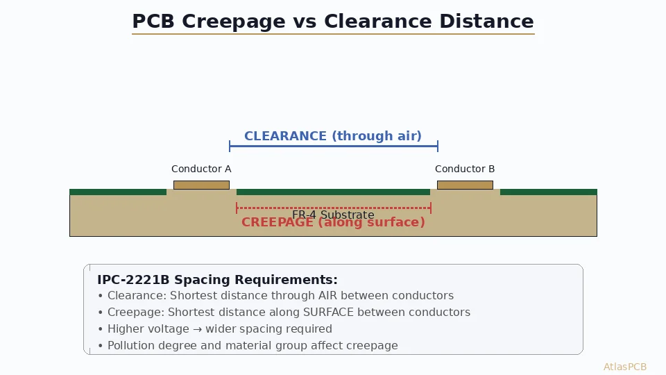
Clearance: Through-Air Distance
Definition and Physics
Clearance is the shortest distance through air between two conductive parts. Air has a dielectric strength of approximately 3 kV/mm at sea level and standard pressure (101.3 kPa, 25°C), but this value drops significantly with:
- Reduced pressure (altitude)
- Increased humidity causing partial discharge
- Non-uniform electric fields (sharp edges concentrate fields)
IPC-2221B Table 6.1 provides minimum clearance values based on:
- Peak operating voltage (DC or AC peak, not RMS)
- Whether conformal coating is applied
- Board condition (internal vs. external layers)
IPC-2221B Clearance Requirements (Key Values)
| Peak Voltage (V) | Bare Board External (mm) | Conformal Coated (mm) | Internal Layers (mm) |
|---|---|---|---|
| 0–15 | 0.1 | 0.05 | 0.05 |
| 16–30 | 0.1 | 0.05 | 0.05 |
| 31–50 | 0.6 | 0.13 | 0.13 |
| 51–100 | 0.6 | 0.13 | 0.13 |
| 101–150 | 0.6 | 0.4 | 0.4 |
| 151–170 | 1.25 | 0.4 | 0.4 |
| 171–250 | 1.25 | 0.4 | 0.4 |
| 251–300 | 1.25 | 0.4 | 0.4 |
| 301–500 | 2.5 | 0.8 | 0.8 |
Note: These values assume sea-level conditions. For high-altitude applications, apply the altitude correction factor from IPC-2221B Section 6.3.
The Altitude Factor
Air becomes thinner at altitude, reducing its insulating capability. The correction factor follows:
$$K_{alt} = e^{1.312 \times 10^{-4} \times (h - 2000)}$$
Where h is altitude in meters (applies only above 2,000 m). Practical multipliers:
- 3,000 m: 1.14×
- 4,000 m: 1.29×
- 5,000 m: 1.48×
- 10,000 m (aircraft cabin): 2.81×
For avionics operating at depressurized altitudes (up to 15,000 m in some military platforms), the required clearances can be 5–10× those at sea level.
Creepage: Along-Surface Distance
Definition and Tracking Phenomenon
Creepage is the shortest distance along the surface of insulating material between two conductors. Surface contamination — dust, moisture, ionic residues from manufacturing — creates partial conductive paths. Over time, repeated partial discharge events carbonize the surface material, creating permanent conductive tracks (called tracking).
The Comparative Tracking Index (CTI) of the base material determines its resistance to tracking:
| Material Group | CTI Range (V) | Examples |
|---|---|---|
| I | ≥ 600 | Ceramic, glass, PTFE |
| II | 400–599 | High-performance FR-4, polyimide |
| IIIa | 175–399 | Standard FR-4, most PCB laminates |
| IIIb | 100–174 | Low-grade phenolic |
Most standard FR-4 laminates fall in Material Group IIIa (CTI 175–399), which significantly impacts required creepage distances.
Pollution Degree
The IEC 60664-1 pollution degree describes the expected contamination environment:
- PD1 — No pollution or only dry, non-conductive pollution (sealed enclosures)
- PD2 — Normally non-conductive pollution, but occasional temporary conductivity due to condensation (most electronics)
- PD3 — Conductive pollution or dry non-conductive pollution that becomes conductive due to condensation (industrial environments)
Creepage Distance Table (per IEC 60664-1)
For Material Group IIIa (standard FR-4), Pollution Degree 2:
| Working Voltage RMS (V) | Creepage (mm) |
|---|---|
| ≤ 50 | 0.6 |
| 100 | 1.0 |
| 150 | 1.6 |
| 200 | 2.0 |
| 250 | 2.5 |
| 300 | 3.2 |
| 400 | 4.0 |
| 600 | 6.3 |
| 1000 | 10.0 |
These values increase significantly for PD3 or Material Group IIIb materials.

Need High-Voltage PCBs with Certified Spacing?
AtlasPCB manufactures boards meeting IPC-2221B and IEC 60664-1 spacing requirements with full DFM verification.
Get a Quote →Practical Design Techniques
1. Slot Isolation for Creepage Enhancement
When board space is tight, routing a slot (routed channel) between high-voltage and low-voltage sections effectively increases the creepage path. A 1 mm wide slot forces the creepage path to go around the slot edges, often adding 3–5 mm of effective creepage distance using minimal board area.
Design rules for slots:
- Minimum slot width: 1.0 mm (manufacturing limit for most fabs)
- Slot length should extend at least 2 mm beyond the conductors on each end
- Avoid placing vias within 0.5 mm of slot edges (mechanical stress)
- Mark slots clearly in fabrication notes
2. Conformal Coating Impact
Conformal coating dramatically reduces required clearance (by 50–75%) because it:
- Prevents condensation from forming direct paths
- Blocks contamination from settling on board surfaces
- Increases the effective CTI of the surface
However, conformal coating does not reliably reduce creepage requirements in most safety standards. UL 60950 and IEC 62368-1 only allow coating to reduce clearance, not creepage, unless the coating is qualified per specific tests.
3. Solder Mask as Insulation
IPC-2221B allows solder mask to be counted as insulation for reducing internal clearance requirements when:
- Solder mask thickness ≥ 12 µm over copper edges
- Applied with verified coverage (no pinholes or skip areas)
- Material is listed for the voltage class
However, solder mask alone does NOT qualify as supplementary or reinforced insulation for safety-critical isolation boundaries (e.g., mains-to-SELV isolation in power supplies).
4. Keepout Zones and Design Rules
Set up your EDA tool with proper spacing rules:
# Example Altium/KiCad rule structure
Rule: HV_Clearance_Primary_to_Secondary
  Scope: Net_Class('PRIMARY') to Net_Class('SECONDARY')
  Clearance: 6.4mm  (for 300V working, reinforced insulation)

Rule: HV_Creepage_Primary_to_Secondary
  Scope: Net_Class('PRIMARY') to Net_Class('SECONDARY')
  Creepage: 8.0mm  (FR-4 Group IIIa, PD2, 300V)
5. Conductor Geometry Considerations
Sharp edges and points concentrate electric fields, reducing effective breakdown voltage:
- Round all high-voltage copper features with ≥ 0.25 mm radius
- Avoid acute-angle traces near high-voltage nets
- Use teardrop pads to eliminate stress concentration points
- Guard rings at ground potential can shape the field distribution
Safety Standard Cross-Reference
Different product safety standards impose additional requirements beyond IPC-2221B:
| Standard | Application | Key Difference |
|---|---|---|
| IEC 62368-1 | IT/AV equipment | Reinforced insulation = 2× basic spacing |
| IEC 60601-1 | Medical devices | 2× MOPP requires 8 mm creepage at 250 VAC |
| IEC 61800-5-1 | Motor drives | Accounts for PWM voltage peaks |
| IEC 60664-1 | General low-voltage | Foundation standard for creepage/clearance |
| UL 61010-1 | Lab equipment | Additional requirements for transient voltage |
For medical or aerospace PCBs, the safety standard requirements always supersede the base IPC-2221B values. Design to the most stringent applicable standard.
Common Design Mistakes
Mistake 1: Measuring clearance center-to-center instead of edge-to-edge. Clearance and creepage are always measured from the nearest edges of conductors, including any solder, tinning, or plating that extends the conductive area.
Mistake 2: Ignoring the solder fillet. A through-hole solder joint extends the conductor by 1–2 mm beyond the pad edge. Include this in your spacing calculations.
Mistake 3: Forgetting about component bodies. A metal heatsink tab, exposed pad, or component lead creates additional conductive surfaces that must maintain spacing from other nets.
Mistake 4: Via-under-component violations. Vias under high-voltage components can create clearance violations on the opposite board layer. Always check spacing on all layers.
Mistake 5: Not accounting for mechanical tolerances. Board edge, slot, and hole position tolerances (typically ±0.1 mm) reduce effective spacing. Subtract worst-case tolerance from your nominal spacing.
Verification and Testing
DFM Verification
Before releasing Gerber files, verify spacing with:
- DRC rules set to the exact voltage/standard requirements
- 3D cross-section analysis at critical boundaries
- IPC-9592 power conversion electronics spacing check
Production Testing
- Hi-pot (dielectric withstand): Apply test voltage (typically 2× working + 1000V or per applicable standard) between isolated networks for 60 seconds
- Insulation resistance: Measure ≥ 100 MΩ at 500 VDC between isolated circuits
- Partial discharge testing: For voltages > 1 kV, verify no partial discharge below rated voltage
Further Reading
- High-Voltage PCB Design Guide
- PCB Power Integrity and PDN Design
- EMI Shielding with Via Fencing
- Signal Integrity Fundamentals
Designing a high-voltage PCB and need help with spacing verification? AtlasPCB provides full DFM review including IPC-2221B and IEC 60664-1 spacing validation as part of every fabrication order. Request a quote to get started.
About AtlasPCB — We specialize in complex PCB manufacturing for HDI, RF, and high-reliability applications. Explore our full PCB manufacturing capabilities . Every order includes free engineering review. Get your quote.
Reviewed by AtlasPCB Engineering Team — IPC-certified manufacturing specialists with 15+ years of production experience in HDI, RF, and high-reliability PCB fabrication. Content based on factory floor data and real customer design reviews.
- ipc-2221b
- creepage
- clearance
- high-voltage
- pcb-design
- safety
- spacing
- standards