· AtlasPCB Engineering · Engineering · 7 min read
PCB Design for EMC Pre-Compliance: Near-Field Probing, Common-Mode Filtering, and Layout Techniques to Pass FCC/CISPR Tests First Time
Master EMC pre-compliance testing at the PCB level. Learn near-field probing techniques, common-mode noise mitigation, clock routing strategies, and layout best practices that reduce radiated emissions before formal testing.
Why Pre-Compliance Matters
Formal EMC testing in an accredited semi-anechoic chamber costs $3,000–$10,000 per test session. A single FCC or CE mark failure typically adds 4–8 weeks to a product schedule as the team debugs, re-spins the PCB, and retests. For startups and hardware companies with tight launch windows, this delay is devastating.
Pre-compliance testing at the PCB level identifies emission problems early—during prototype bring-up—when fixes are cheap (firmware register changes, component additions, shield placement) rather than requiring board re-spins.
This guide covers the complete pre-compliance workflow from equipment selection through systematic debugging to design rule implementation that virtually guarantees first-time compliance.

EMC Emission Fundamentals for PCB Designers
Radiation Mechanisms at PCB Level
PCBs don’t radiate like intentional antennas—they’re accidentally efficient radiators through three mechanisms:
Differential-mode radiation: Current flowing in a signal-return loop creates a magnetic dipole. Radiation intensity proportional to loop area × frequency² × current.
Common-mode radiation: Identical currents on both conductors of a cable (or across a PCB-chassis boundary) create an electric monopole. Even microamps of CM current at GHz frequencies produce significant radiation because the “antenna” (cable) is electrically long.
Slot antenna effects: Gaps in ground planes, connector cutouts, and board edges create slot radiators that are efficient at frequencies where slot length ≈ λ/2.
Common-Mode Dominance
In practical products, common-mode radiation accounts for 80–90% of emission failures. A 5 µA common-mode current at 300 MHz on a 1-meter cable exceeds FCC Class B limits. Differential-mode radiation is secondary because PCB trace loops are small relative to wavelength.
This means: EMC compliance is primarily a common-mode noise problem, not a signal integrity problem. Your signals can have perfect eye diagrams while still causing emission failures.
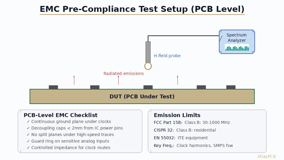
Pre-Compliance Test Equipment and Setup
Near-Field Probes
| Probe Type | Detects | Use Case |
|---|---|---|
| H-field loop (20mm) | Magnetic field, current flow | Identifying noisy traces, IC activity |
| H-field loop (5mm) | Localized current hotspots | Pin-level diagnosis |
| E-field tip | Electric field, voltage nodes | Connector emissions, slot antennas |
Technique: Scan the probe 1–3mm above the PCB surface while monitoring the spectrum analyzer. Move slowly and note where specific frequency peaks appear or disappear.
Interpreting Spectrum Analyzer Results
What you see:
- Clock harmonics (crystal oscillator × N): Sharp spectral peaks at integer multiples of the fundamental. Strongest source of narrowband emissions.
- Switching regulator fundamentals: Broad peaks at fsw (typically 500 kHz–3 MHz) and harmonics to 200+ MHz
- Digital broadband: Wideband floor elevation from high-speed buses (DDR, PCIe, USB)
- Resonances: Peaks that appear only at specific probe positions (cavity/slot modes)
Correlation to Far-Field Limits
Near-field probing gives relative measurements (dBµV into 50Ω), not absolute far-field levels. Use these empirically-derived guidelines:
- If a near-field H-probe reading exceeds -10 dBm at 3mm distance, the associated trace/IC will likely contribute to a far-field limit exceedance
- A 20 dB reduction in near-field reading typically provides 15–20 dB far-field improvement
- Focus on the 5 highest peaks in your near-field scan—these correlate to formal test failures
Systematic PCB Design Rules for EMC
Rule 1: Continuous Ground Plane Under All Clocks
The single most important EMC design rule: never break the ground plane beneath clock signals or high-frequency traces.
Every signal requires a return current path. At high frequencies, return current flows directly beneath the signal trace on the nearest reference plane. If that plane is interrupted (split, void, slot), the return current detours around the gap—creating a large loop that radiates efficiently.
Implementation:
- No power plane splits under clock routing areas
- No through-hole component leads creating plane voids in clock regions
- Dedicated clock routing areas with solid, uninterrupted ground reference
- Return path vias adjacent to every layer transition of high-speed signals
Rule 2: Decoupling Capacitor Placement
Target: < 2mm from IC power pin to cap, with return via within 1mm of cap ground pad.
Why location matters: at 500 MHz, a 0402 capacitor’s self-resonant frequency is ideal, but 5mm of trace inductance (≈3 nH) renders the cap ineffective above 200 MHz. Proximity is everything.
Tiered decoupling strategy:
- Tier 1 (0201/0402, 100nF): One per power pin, < 2mm
- Tier 2 (0402/0603, 1µF): One per 2–4 power pins, < 5mm
- Tier 3 (0805/1206, 10–47µF): Bulk capacitance per power rail, < 15mm
Rule 3: Clock Source Containment
Crystal oscillators and PLL outputs are the highest-risk EMI sources:
- Route clock traces on inner layers (stripline) whenever possible—enclosed between two ground planes, no radiation
- If microstrip is unavoidable, keep clock traces ≥ 200 mil from board edge
- Guard traces with ground stitching vias on both sides of clock routes
- Spread-spectrum clocking (SSC): 0.5–1.5% modulation reduces clock harmonics by 6–12 dB with minimal SI impact
Rule 4: I/O Connector EMC
Cables attached to I/O connectors are the primary radiation antennas. Treat every connector as an EMC boundary:
- Common-mode chokes on every cable interface (USB, HDMI, Ethernet, power)
- Ground plane continuous to connector shell: No plane void between IC ground and connector ground
- Ferrite beads on I/O power lines to prevent HF noise coupling
- Shield grounding: 360° contact between cable shield and connector shell (no pigtail ground wires)
Rule 5: Board Edge Management
Board edges are efficient slot radiators:
- Keep high-speed traces ≥ 3× trace width from board edge (minimum 40 mil)
- Ground plane stitching vias along board perimeter at λ/20 spacing (< 5mm for 3 GHz compliance)
- No traces running parallel to board edge without ground guard
- Connector placement: I/O connectors on one board edge with dedicated ground pour
Need EMC-Optimized PCB Manufacturing?
AtlasPCB provides controlled-impedance boards with precise ground plane construction critical for EMC compliance. We review your stackup for EMC best practices.
Start Your Design Review →Advanced EMC Techniques
Common-Mode Filter Design
For cables that fail conducted or radiated limits:
CM choke selection criteria:
- Impedance > 100Ω at the problem frequency
- Differential impedance < 1Ω (minimal signal impact)
- Current rating sufficient for the application
- Self-resonant frequency above the highest problem harmonic
Placement: As close to the connector as physically possible. CM noise between the IC and choke still radiates from board traces—the choke only prevents cable radiation.
Split Power Plane Management
When split power planes are unavoidable:
- Bridge capacitors: Place 10–100nF capacitors across every power split boundary at ≤ 5mm spacing
- Signal routing: Never route high-speed signals across a power split boundary
- Alternative: Use a full ground plane on an adjacent layer as the return reference, accepting slightly higher impedance
Spread-Spectrum Clock Modulation
SSC (Spread-Spectrum Clocking) is the most cost-effective EMI reduction technique:
- 0.5% center-spread: ~6 dB harmonic reduction
- 1.0% down-spread: ~10 dB harmonic reduction
- Applicable to: HDMI, USB, PCIe, DDR (most interfaces tolerate SSC)
- Caution: Not suitable for ADC/DAC clocks, RF synthesizers, or timing-critical interfaces
PCB-Level Shielding
When layout optimization alone is insufficient:
- Board-level shields (stamped metal cans) over noisy ICs: 20–40 dB attenuation
- Embedded shielding layers: Internal copper pour connected to ground with via fence
- Compartmentalization: Separate analog, digital, and RF sections with ground stitching boundaries
Pre-Compliance Testing Workflow
Step 1: Baseline Scan
Before any modifications:
- Power the board with all systems active
- Scan with H-field probe over entire board surface
- Record peak frequencies and locations
- Compare peaks to clock frequencies and their harmonics
- Identify the top 5 emission sources
Step 2: Root-Cause Identification
For each identified hotspot:
- Trace the emission path from source IC to radiation point
- Check for: missing decoupling, ground plane void, layer transition without return via
- Map the current return path—where is the loop area large?
Step 3: Iterative Fix and Verify
Apply fixes in order of expected impact:
- Add missing decoupling capacitors (easiest, most common fix)
- Add common-mode chokes on cable interfaces
- Add ground stitching vias near high-speed transitions
- Enable spread-spectrum on applicable clocks
- Add board-level shields as last resort
Re-scan after each modification to verify improvement and avoid masking other issues.
Step 4: Final Verification
Before formal testing:
- All near-field peaks should be > 6 dB below your informal correlation limit
- Test with final cables, enclosure, and power supply (packaging matters!)
- Test worst-case operating mode (maximum bus activity, all I/O connected)
PCB DFM for EMC: Fabrication Specifications
These PCB specifications directly impact EMC performance:
| Parameter | EMC-Critical Specification |
|---|---|
| Ground plane voiding | ≤ 5% void area under signal regions |
| Via drill accuracy | ±2 mil (for return path via alignment) |
| Impedance tolerance | ±7% (prevents reflection/re-radiation) |
| Copper roughness | HVLP preferred (reduces skin-effect loss, lower thermal noise) |
| Layer-to-layer registration | ±3 mil (maintains reference plane overlap) |
| Soldermask adhesion | IPC Class 2 min (prevents galvanic corrosion of ground connections) |
Further Reading
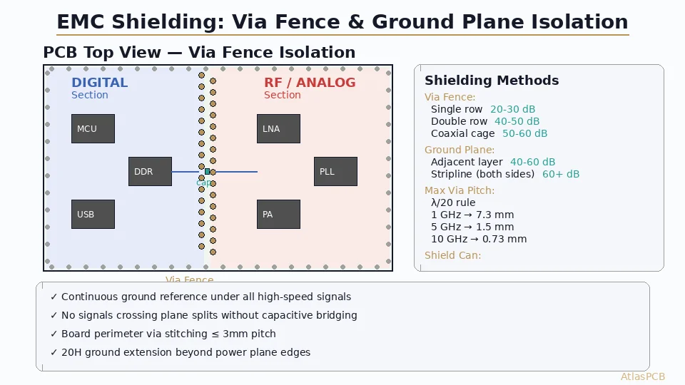
- EMC Shielding: Via Fencing and Ground Planes
- PCB Grounding Techniques
- Power Integrity and PDN Decoupling Design
- High-Voltage PCB Design: Creepage and Clearance
Designing for EMC compliance from the start? AtlasPCB manufactures controlled-impedance boards with tight registration tolerance and minimal ground plane voiding—the fabrication foundation for passing FCC/CE testing first time. Request a quote or review our PCB capabilities.
About AtlasPCB — We specialize in complex PCB manufacturing for HDI, RF, and high-reliability applications. Explore our impedance-controlled PCB manufacturing . Every order includes free engineering review. Get your quote.
Reviewed by AtlasPCB Engineering Team — IPC-certified manufacturing specialists with 15+ years of production experience in HDI, RF, and high-reliability PCB fabrication. Content based on factory floor data and real customer design reviews.
- EMC
- pre-compliance
- FCC Part 15
- CISPR 32
- radiated emissions
- near-field probe
- PCB layout