· AtlasPCB Engineering · Engineering · 10 min read
PCB Design for Edge AI Inference Modules: HDI, Thermal, and Signal Integrity
Complete design guide for edge AI inference module PCBs — covering HDI stackup requirements for 0.4-0.65mm BGA escape, thermal via arrays for 5-25W dissipation in compact form factors, DDR4/5 and high-speed SerDes routing, and material selection that balances performance with cost.
Typical Edge AI Module Requirements at a Glance
Before diving into design details, here is what a representative edge AI inference module demands from the PCB:
| Parameter | Typical Range | Notes |
|---|---|---|
| AI SoC package | BGA, 0.4-0.65mm pitch | WLCSP on some low-power parts |
| Layer count | 8-12 | HDI required for 0.5mm pitch and below |
| Board thickness | 1.0-1.6mm | Thinner for module-on-carrier designs |
| Power dissipation | 5-25W | Fanless thermal budget typical |
| Memory interface | DDR4/LPDDR4X/DDR5 | 2-4 channels, 32-64 bit |
| High-speed SerDes | PCIe Gen3/4, MIPI CSI-2/DSI | 5-16 Gbps per lane |
| Operating temp | -20 to +85C (industrial) | Extended for automotive |
| Key materials | High-Tg FR-4 (Tg 170C+) | Low-loss only for 25G+ links |
This combination of fine-pitch BGAs, aggressive thermal constraints, and mixed high-speed interfaces makes edge AI one of the most demanding categories for PCB design below server-grade.
HDI Requirements: Why Edge AI Needs Microvias
The BGA Escape Problem
Edge AI processors from vendors like NVIDIA (Jetson series), Qualcomm (QCS/QRB), Hailo, and various RISC-V AI accelerators use BGA packages with 0.4-0.65mm ball pitch. At 0.5mm pitch, the inner rows of a 15x15mm BGA simply cannot escape on surface layers alone — there is no room for traces between pads using conventional through-hole vias.
The math is straightforward:
- 0.5mm pitch = 500um center-to-center
- BGA pad diameter: 250-280um (typical for 0.5mm pitch)
- Remaining gap between pads: 220-250um
- A through-hole via with 0.3mm drill + 0.5mm pad consumes the entire gap
Microvias (0.075-0.1mm laser drill, 0.2-0.25mm pad) solve this. A via-in-pad microvia beneath each BGA ball routes the signal to an inner layer where trace routing is unconstrained by pad geometry.
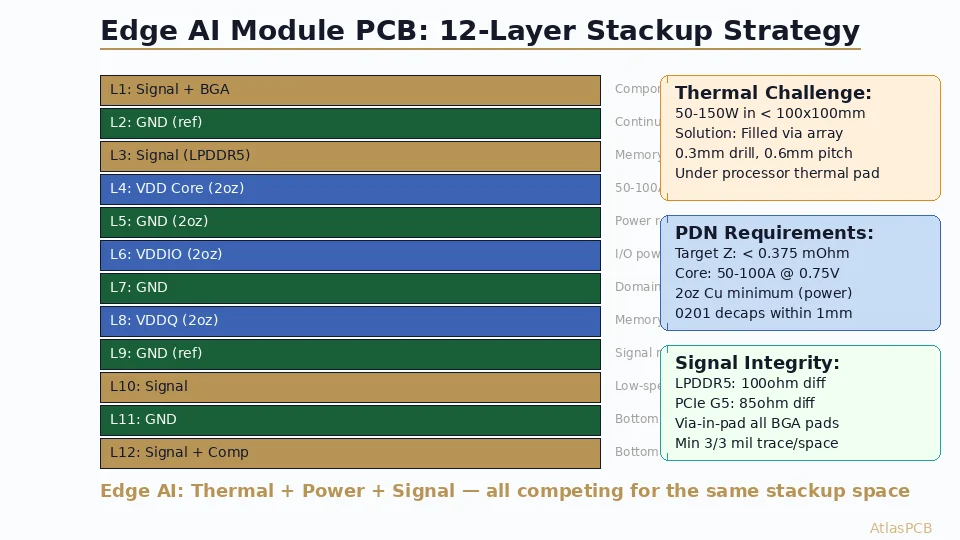
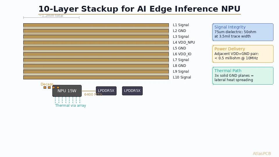
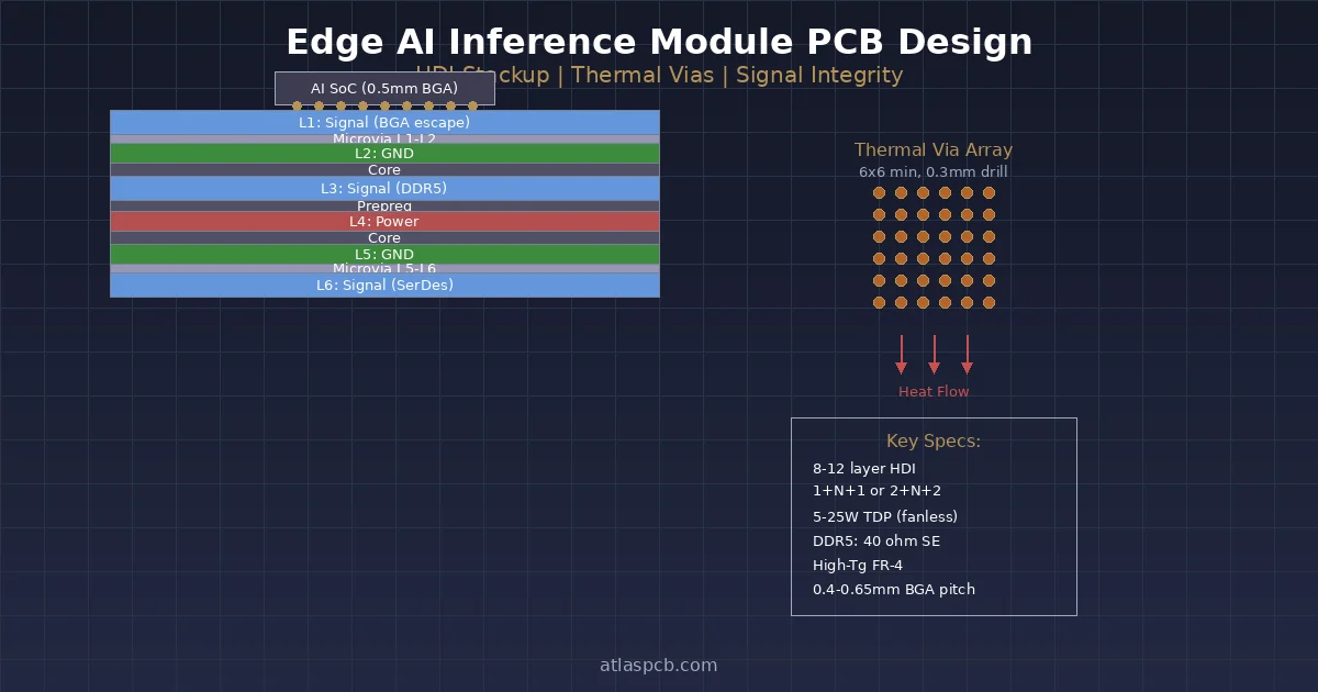
Stackup Architecture for Edge AI
For a typical 10-layer 2+N+2 HDI stackup:
L1 - Signal/Component (microvia L1→L2)
L2 - Ground (microvia L2→L3)
L3 - Signal (high-speed routing)
L4 - Power
L5 - Ground
L6 - Signal
L7 - Power
L8 - Signal (high-speed routing)
L9 - Ground (microvia L9→L10)
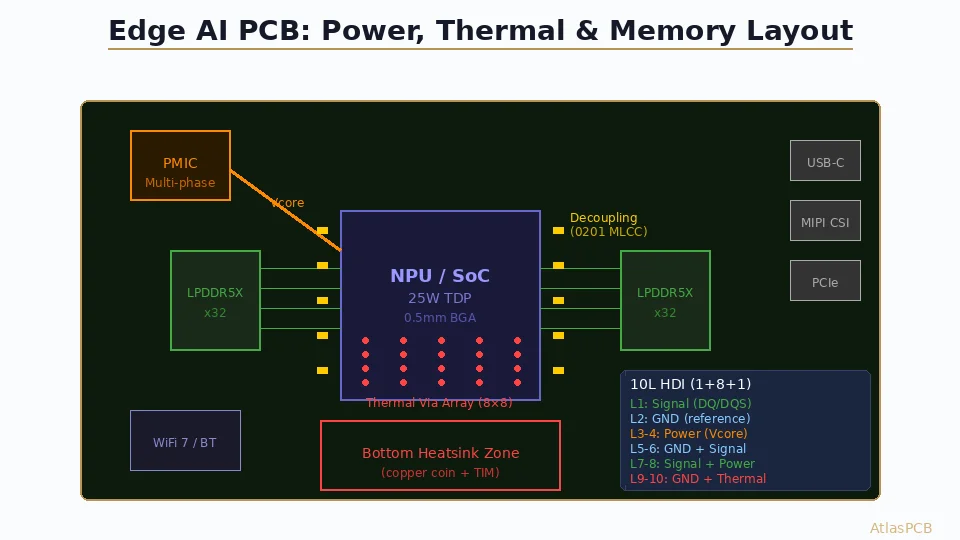
L10 - Signal/Component (microvia L10→L9)This structure provides via-in-pad capability on both sides (important when memory sits opposite the SoC), four controlled-impedance signal layers, and dedicated power/ground plane pairs for PDN performance.
For designs needing only one HDI side (SoC on top, passive components on bottom), a 1+N+1 8-layer stackup reduces cost by 15-25% while still enabling 0.5mm BGA escape.
HDI FABRICATION
Up to 5+N+5 HDI Buildup
Stacked and staggered microvias, via-in-pad, 0.075mm laser drill. Built for BGA escape density.
Quote Your HDI Design ›Thermal Management: 5-25W in a Compact Form Factor
The Thermal Challenge
Edge AI modules are defined by their thermal contradiction: server-class compute density in form factors that preclude active cooling. A 15W AI SoC in a 15x15mm package produces roughly 6.7 W/cm2 — comparable to laptop CPUs but in enclosures designed for fanless or minimal-airflow operation.
The PCB is not just an electrical interconnect; it is a primary thermal path. Effective thermal design at the board level determines whether the product throttles under sustained inference loads.
Thermal Via Array Design
The exposed thermal pad on the bottom of most AI SoCs requires a via array connecting it to internal copper planes and the opposite-side heat spreader:
Minimum viable thermal via array:
- Grid: 6x6 (36 vias minimum for 10-15W)
- Drill diameter: 0.3mm
- Via pitch: 0.6mm (center-to-center)
- Copper fill: plated, no tenting (maximizes thermal conductivity)
- Target thermal resistance: 12-18 W/mK through-board
High-performance array (15-25W):
- Grid: 8x8 or larger (64+ vias)
- Consider via-in-pad with copper fill for maximum conductivity
- 2oz copper on thermal relief layer (L2 or internal ground)
- Back-side exposed copper pad for heatsink attach
Copper Pour Strategy
Beyond the via array, internal copper planes serve as lateral heat spreaders:
- Maintain unbroken ground/power planes under the SoC footprint (no splits, minimal routing)
- Use 2oz copper on at least one internal plane in the thermal path
- Keep thermal relief connections to mounting pads — do not use full flood relief patterns that restrict heat flow
- Route high-speed signals on layers NOT adjacent to the primary thermal plane to avoid coupling with thermal structures
The combination of thermal via array + 2oz internal copper + back-side heatsink pad typically achieves junction-to-ambient thermal resistance of 8-15 C/W in still air — sufficient for 15-20W at 85C ambient with 100-105C junction limit.
Signal Integrity: DDR and High-Speed SerDes
DDR4/5 Routing for AI Memory Bandwidth
Edge AI processors are memory-bandwidth hungry. A typical inference workload streams activation data continuously from DRAM. Routing DDR4/5 interfaces correctly is non-negotiable for reliable operation.
DDR4 (3200 MT/s) key parameters:
- Single-ended impedance: 40 ohm (DQ, DQS, Address)
- Trace width: ~4.5mil on 4mil dielectric (High-Tg FR-4)
- Length matching within byte lane: +/-2.5mm
- Address/command group matching: +/-5.0mm
- Via stub length limit: not critical at DDR4 speeds
DDR5/LPDDR5X (6400+ MT/s) key parameters:
- Single-ended impedance: 40 ohm (+/-10% tolerance — tighter than DDR4)
- Differential impedance (clock): 80 ohm
- Trace width: ~3.5-4.0mil on 3.5mil dielectric
- Length matching within byte lane: +/-1.0mm
- Crosstalk spacing: minimum 3x trace width between groups
- Via stub effect becomes relevant — use microvias or backdrilling for memory vias
The move from DDR4 to DDR5/LPDDR5X roughly doubles the routing difficulty: tighter impedance tolerance, stricter length matching, and via stubs that were acceptable at 3.2 GHz cause measurable eye degradation at 6.4 GHz.
High-Speed SerDes: PCIe and MIPI
Edge AI modules commonly use PCIe Gen3/Gen4 for host communication and MIPI CSI-2 for camera sensor input:
PCIe Gen3 (8 GT/s):
- Differential impedance: 85 ohm
- Maximum trace loss budget: 8 dB at 4 GHz (Nyquist)
- Standard High-Tg FR-4 supports 150-200mm trace length at this speed
- Via transitions: max 2 layer transitions per link
PCIe Gen4 (16 GT/s):
- Differential impedance: 85 ohm
- Maximum trace loss budget: 8 dB at 8 GHz
- High-Tg FR-4 limits trace length to 75-100mm
- Backdrilling or microvias required to eliminate via stubs
- Consider low-loss prepreg on signal layers if trace length exceeds 100mm
MIPI CSI-2 (up to 4.5 Gbps/lane, C-PHY at 5.7 Gsps/trio):
- D-PHY: 80-100 ohm differential
- C-PHY: characteristic impedance per trio, layout-sensitive
- Short traces (typically under 50mm) — FR-4 is never the limitation
- Maintain pair symmetry and minimize length mismatch within each lane
SIGNAL INTEGRITY
Impedance-Controlled Fabrication
3/3mil trace/space, controlled impedance +/-10%, TDR-verified. Built for high-speed edge AI designs.
Request Stackup Review ›Power Delivery: Multi-Rail PMICs and Decoupling
The Multi-Rail Challenge
A typical edge AI SoC requires 5-8 distinct voltage rails:
- Core logic: 0.7-0.9V at 10-20A (highest current, tightest regulation)
- Memory I/O: 1.1V (DDR4) or 1.0V (DDR5) at 2-5A
- I/O banks: 1.8V and 3.3V at 1-3A each
- PLL/analog: 0.8-1.0V at 100-500mA (lowest noise requirement)
- NPU/accelerator: 0.75-0.85V at 5-15A (separate from CPU core for DVFS)
Modern edge AI designs use integrated PMICs (Power Management ICs) that provide multiple rails from a single chip, reducing component count and board area. However, the PCB power delivery network (PDN) between PMIC output and SoC power pins remains critical.
PDN Design Rules for Edge AI
Core voltage rail (highest priority):
- Target PDN impedance: under 1 milliohm from DC to 100 MHz
- Use wide, short power plane shapes — minimize via transitions between PMIC and SoC
- Place PMIC within 10mm of SoC power pins when possible
- Bulk capacitance: 4-6x 22uF MLCC (0402/0603) within 3mm of power pins
- High-frequency decoupling: 10-20x 100nF 0201 directly adjacent to BGA power via clusters
Decoupling capacitor placement strategy:
- 0201 100nF caps: immediately adjacent to power/ground via pairs at BGA perimeter (0.5-1.0mm from via)
- 0402 1uF caps: next ring, 1-3mm from BGA edge
- 0603/0805 22uF bulk caps: 3-8mm from BGA, connected with short, wide traces to power plane
Common mistake to avoid: Routing power through narrow necked-down traces between BGA pads to reach decoupling caps. Every milliohm of trace resistance in the power path degrades transient response. Use inner-layer power planes for distribution and via arrays for vertical transitions.
Material Selection: When Standard FR-4 Is Enough
One of the most common over-engineering mistakes in edge AI PCB design is specifying exotic low-loss laminates when High-Tg FR-4 performs adequately.
High-Tg FR-4 (Tg 170C+, such as IT180A or S1000-2M):
- Dk: 4.2-4.4 at 1 GHz
- Df: 0.018-0.022 at 1 GHz
- Supports DDR5 at 6400 MT/s on traces under 40mm (typical for edge modules)
- Supports PCIe Gen3 on traces under 200mm
- Supports PCIe Gen4 on traces under 100mm
- Cost baseline: 1x
Mid-loss laminate (such as EM-370D or Megtron-4):
- Dk: 3.8-4.0 at 1 GHz
- Df: 0.008-0.012 at 1 GHz
- Only justified when PCIe Gen4 traces exceed 100mm or DDR5 traces exceed 50mm
- Cost premium: 1.3-1.5x
Decision rule: If your longest high-speed trace is under 75mm and maximum signaling rate is 16 GT/s, standard High-Tg FR-4 works. Most edge AI modules — being physically compact (40-70mm board dimension) — never need anything beyond standard material.
For boards requiring mixed materials (e.g., one signal layer pair on low-loss prepreg for a long PCIe Gen4 link, rest on standard), hybrid stackup construction is available but adds 20-40% to fabrication cost due to the additional lamination cycle.
Design-for-Manufacturing Tips for Edge AI Boards
Via-in-Pad Requirements
Edge AI boards with 0.4-0.5mm BGA pitch almost universally require via-in-pad with copper fill and planarization:
- Specify VIPPO (Via-In-Pad Plated Over): laser-drilled microvia, copper-filled, cap-plated, and planarized to less than 1mil (25um) dimple
- This enables direct BGA soldering on the via without voiding
- AtlasPCB supports VIPPO with dimple control under 25um — verify this specification in your fab notes
Panelization Considerations
Edge AI modules are often small (30-70mm per side) and panelized in arrays of 4-20 boards. Consider:
- Breakaway tab placement away from high-speed connector edges (mechanical stress from depanelization can micro-crack solder joints)
- Add fiducials on the panel frame AND individual boards for pick-and-place registration
- 5-rail scoring or routed tabs — match to your assembly house preference
Test Point Accessibility
For production test and debug:
- DDR interface: provide at least one DQ and one DQS pair accessible on the surface layer for oscilloscope probing
- Power rails: test points on each major rail (accessible from top or bottom) for in-circuit test
- JTAG/SWD: always break out to a header or test pad array — edge AI processors invariably need firmware debug during bring-up
DFM REVIEW
Free Engineering Review for Complex Designs
Submit your edge AI board files for stackup verification, impedance modeling, and manufacturing feasibility check.
Submit for Review ›Putting It Together: Design Checklist
Before releasing an edge AI inference module PCB to fabrication, verify:
- BGA escape: All inner-row balls have microvia escape paths; confirm via-in-pad specification in fab notes
- Thermal: Via array size matches thermal simulation; back-side pad area adequate for heatsink
- Impedance: Stackup impedance modeling matches target values with manufacturing tolerance (+/-10%)
- DDR routing: Length matching within spec; crosstalk spacing maintained through entire route
- SerDes: Via stub length acceptable for target data rate; differential pair symmetry maintained
- PDN: Decoupling placed per strategy above; power plane shapes unbroken under SoC
- Material: Confirm High-Tg FR-4 loss budget is adequate for your trace lengths and data rates
- DFM: Via-in-pad specified, annular ring meets minimum (3mil/75um), acid traps cleaned
Getting these right on the first spin saves 3-6 weeks of respin time — critical in the fast-moving edge AI market where design cycles are measured in months, not years.
ATLASPCB
Ready to Fabricate Your Edge AI Board?
HDI up to 5+N+5, via-in-pad, impedance control, and full DFM review included. 1-day rush available for prototypes.
Get Your Quote ›Related Reading
About AtlasPCB — We specialize in complex PCB manufacturing for HDI, RF, and high-reliability applications. Explore our HDI PCB manufacturing capabilities, impedance-controlled PCB manufacturing, or get an aluminum and metal-core PCB services . Every order includes free engineering review. Get your quote.
Reviewed by AtlasPCB Engineering Team — IPC-certified manufacturing specialists with 15+ years of production experience in HDI, RF, and high-reliability PCB fabrication. Content based on factory floor data and real customer design reviews.
- edge AI
- PCB design
- HDI
- thermal management
- signal integrity
- BGA routing
- DDR5
- impedance control
- inference hardware
- AI module