· Technical Guide · 15 min read
Dynamic Flex PCB Design — Bend Radius, Material Selection, and Reliability
A comprehensive engineering guide to dynamic flex PCB design, covering minimum bend radius formulas, rolled annealed vs electrodeposited copper, adhesiveless constructions, stiffener design, IPC-2223 requirements, fatigue life testing, and real-world applications.
Introduction: Static vs. Dynamic Flex Applications
Flexible printed circuits are broadly categorized into two application classes based on whether the flex region bends during the product’s operational life:
Static flex (flex-to-install) — The circuit bends during assembly but remains fixed once installed. Examples include folding a flex circuit to connect two rigid board sections inside a smartphone, or wrapping a flex around a battery pack. Static flex circuits may endure a few bend cycles during assembly and field service but are not designed for continuous flexing.
Dynamic flex (flex-in-use) — The circuit undergoes repeated bending during normal operation, potentially millions of cycles over the product’s lifetime. Examples include laptop hinge connections, print head cables in inkjet printers, robotic arm cables, and disk drive actuator flex assemblies. Dynamic flex circuits demand fundamentally different design rules, material selections, and reliability validation approaches.
The failure modes differ sharply between the two categories. Static flex failures are typically manufacturing defects — cracked conductors from over-bending during assembly, delamination from improper material handling. Dynamic flex failures are fatigue-driven: copper work-hardening leads to crack initiation and propagation after thousands or millions of cycles, even when the bend radius and strain are within nominal limits.
This guide focuses on dynamic flex design — the material science, geometric constraints, and reliability testing required to ensure long-life operation. For foundational flex PCB design principles, see our flex PCB design guidelines. For designs combining rigid and flex sections, refer to our rigid-flex PCB design guide.
Minimum Bend Radius: The Fundamental Constraint
Why Bend Radius Matters
When a flex circuit bends, the outer surface experiences tensile strain and the inner surface experiences compressive strain. The magnitude of this strain is directly proportional to the material thickness and inversely proportional to the bend radius:
ε = t / (2R)
Where:
- ε = surface strain (dimensionless)
- t = total flex circuit thickness (including copper, adhesive, coverlay, and stiffeners within the bend zone)
- R = bend radius (measured to the inside surface of the bend)
Copper conductors can tolerate limited plastic deformation before fatigue cracking begins. The strain threshold depends on the copper type, grain structure, and number of bend cycles:
- Single bend (static flex): Copper can tolerate strains up to ~1.5–2.0% without cracking
- Dynamic flex (>100,000 cycles): Copper strain must be limited to ~0.1–0.3% to achieve acceptable fatigue life
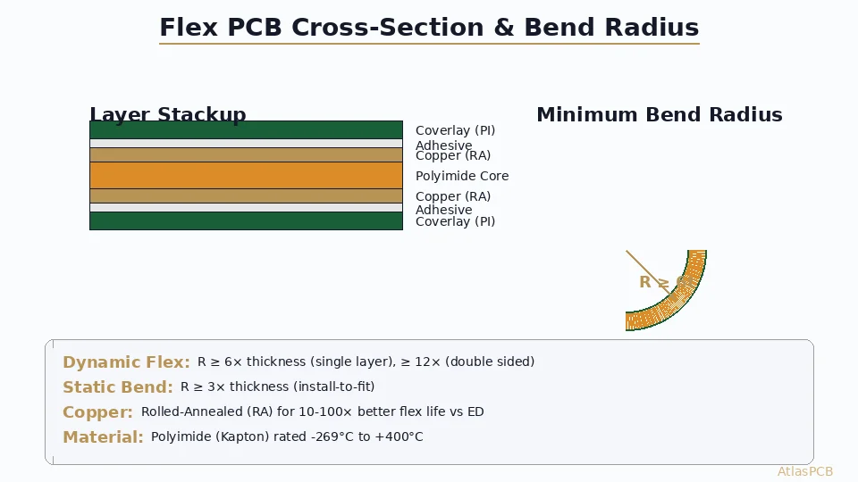
The 6× and 12× Rules
Industry convention distills these strain limits into simple bend radius rules:
Static flex (single bend or flex-to-install):
- Minimum bend radius = 6 × total thickness of the flex assembly in the bend zone
- This yields a surface strain of approximately 8.3% — well within single-bend capability for most copper types
Dynamic flex (repeated bending, >100,000 cycles):
- Minimum bend radius = 12 × total thickness of the flex assembly in the bend zone
- This yields approximately 4.2% surface strain — still aggressive for high-cycle applications
These rules are starting points, not guarantees. For applications requiring millions of cycles (e.g., laptop hinges rated for 20,000+ open/close cycles, or industrial robotic joints), the actual minimum bend radius should be validated through fatigue testing on representative samples.
Bend Radius Calculation Example
Consider a dynamic flex circuit with the following stack-up in the bend zone:
| Layer | Material | Thickness |
|---|---|---|
| Coverlay (top) | Polyimide + adhesive | 25 µm + 25 µm = 50 µm |
| Copper (top) | Rolled annealed copper | 18 µm (½ oz) |
| Base substrate | Polyimide | 25 µm |
| Copper (bottom) | Rolled annealed copper | 18 µm (½ oz) |
| Coverlay (bottom) | Polyimide + adhesive | 25 µm + 25 µm = 50 µm |
| Total | 161 µm |
Applying the 12× rule:
- Minimum dynamic bend radius = 12 × 0.161 mm = 1.93 mm
Rounding up for manufacturing margin: R_min = 2.0 mm
At this radius, the surface strain is:
- ε = 0.161 / (2 × 2.0) = 0.040 = 4.0%
For a target life of >1 million cycles, further derating may be needed — a bend radius of 3.0–4.0 mm (19–25× thickness) would reduce strain to 2.0–2.7%, significantly extending fatigue life.
Factors That Increase Effective Thickness
Designers must account for all materials within the bend zone when calculating total thickness:
- Adhesive layers — Each adhesive bond line adds 12–25 µm
- Stiffeners — Must never extend into the bend zone
- Solder mask — Adds 20–40 µm and may crack during dynamic flexing (use coverlay instead)
- Component leads — Solder joints and component bodies must be kept outside the bend zone
- Plating buildup — Electrolytic plating on pads can add 5–15 µm locally
Copper Selection: Rolled Annealed vs. Electrodeposited
Electrodeposited (ED) Copper
Standard PCB copper foil is produced by electrodeposition — copper is plated from a sulfate bath onto a rotating titanium drum. The resulting foil has a columnar grain structure perpendicular to the foil surface, with grain sizes typically in the 1–5 µm range.
Key characteristics for flex applications:
- Tensile strength: 310–380 MPa (higher than RA copper)
- Elongation at break: 5–12%
- Fatigue life: Limited — columnar grains provide preferential crack propagation paths
- Surface roughness: Higher on the drum side (matte) — good for adhesion but creates stress concentrators
- Cost: Lower than RA copper
- Application: Acceptable for static flex; unsuitable for dynamic flex with >1,000 cycles
Rolled Annealed (RA) Copper
Rolled annealed copper is produced by repeatedly rolling a copper ingot through progressively thinner gaps, followed by annealing (heat treatment at 150–250 °C) to recrystallize the grain structure. The result is a smooth, equiaxed grain structure with grains oriented parallel to the foil surface.
Key characteristics for flex applications:
- Tensile strength: 200–260 MPa (lower than ED copper)
- Elongation at break: 15–30% (significantly higher than ED)
- Fatigue life: 5–10× longer than ED copper at equivalent strain levels
- Surface roughness: Very smooth on both sides — fewer stress concentration points
- Grain orientation: Parallel to the foil surface, resisting crack propagation through the thickness
- Cost: 30–50% premium over ED copper
- Application: Required for all dynamic flex circuits
Grain Structure and Fatigue Mechanism
The fundamental difference is in how cracks initiate and propagate:
ED copper: Columnar grains create grain boundaries that run through the full foil thickness. Under cyclic bending, micro-cracks nucleate at the rough matte surface and propagate along these vertical grain boundaries, reaching through-thickness failure relatively quickly. Typical fatigue life at 0.3% strain: 10,000–50,000 cycles.
RA copper: Equiaxed, horizontally oriented grains present a tortuous path for crack propagation. Cracks must change direction at each grain boundary, requiring significantly more energy to propagate through the thickness. Typical fatigue life at 0.3% strain: 100,000–500,000+ cycles.
For critical dynamic flex applications, specify RA copper explicitly on the fabrication drawing. Note that RA copper is typically available only in standard thicknesses: 9 µm (¼ oz), 12 µm (⅓ oz), 18 µm (½ oz), and 35 µm (1 oz). Use the thinnest copper that meets electrical requirements — ½ oz (18 µm) is the most common choice for dynamic flex.
Adhesiveless Constructions
The Problem with Adhesive Layers
Traditional flex circuits bond copper foil to a polyimide substrate using acrylic or epoxy adhesive layers, each 12–25 µm thick. In dynamic flex applications, adhesive layers present several problems:
- Added thickness — Each adhesive layer increases the total flex thickness, directly increasing the minimum bend radius
- Differential CTE — Acrylic adhesives have a coefficient of thermal expansion (CTE) of 80–100 ppm/°C, compared to 20 ppm/°C for polyimide and 17 ppm/°C for copper. This CTE mismatch creates internal stresses during thermal cycling
- Delamination risk — Under repeated flexing, adhesive layers can delaminate, especially at elevated temperatures where adhesive bond strength decreases
- Z-axis moisture absorption — Adhesive layers absorb moisture more readily than polyimide, potentially causing delamination during reflow (popcorn effect)
Adhesiveless (Cast) Polyimide Laminates
Adhesiveless flex laminates are produced by casting a polyimide precursor solution directly onto the copper foil, then curing at high temperature (>300 °C) to form a polyimide film bonded directly to the copper. No adhesive layer is present.
Benefits for dynamic flex:
| Parameter | Adhesive-Based | Adhesiveless |
|---|---|---|
| Total thickness (2-layer, ½ oz Cu) | ~130 µm | ~80 µm |
| Minimum dynamic bend radius | ~1.6 mm | ~1.0 mm |
| Temperature rating | 105–130 °C | 200–250 °C |
| Copper peel strength | 0.8–1.2 N/mm | 0.7–1.0 N/mm |
| CTE compatibility | Poor | Excellent |
| Moisture absorption | Higher | Lower |
| Cost premium | Baseline | +20–40% |
Major adhesiveless laminate brands include DuPont Pyralux AP, Panasonic Felios, and Nippon Steel Chemical ESPANEX.
For dynamic flex designs, adhesiveless construction is strongly recommended. The reduction in total thickness alone can decrease the minimum bend radius by 30–40%, and the improved CTE matching and thermal stability significantly enhance long-term reliability.
Stiffener Design for Dynamic Flex
Purpose of Stiffeners
Stiffeners are rigid or semi-rigid materials bonded to the flex circuit in areas that require mechanical support — typically component mounting areas, connector interfaces, and mounting points. In dynamic flex designs, stiffeners serve the additional critical function of defining the bend zone boundaries.
Stiffener Materials
| Material | Thickness Range | Key Properties |
|---|---|---|
| FR-4 | 0.2–1.6 mm | Low cost, easy to process, compatible with solder reflow |
| Polyimide | 0.075–0.5 mm | Good for thin profiles, excellent temperature resistance |
| Stainless steel | 0.1–0.3 mm | High stiffness, EMI shielding, precise thickness control |
| Aluminum | 0.3–1.0 mm | Heat dissipation, moderate stiffness, lightweight |
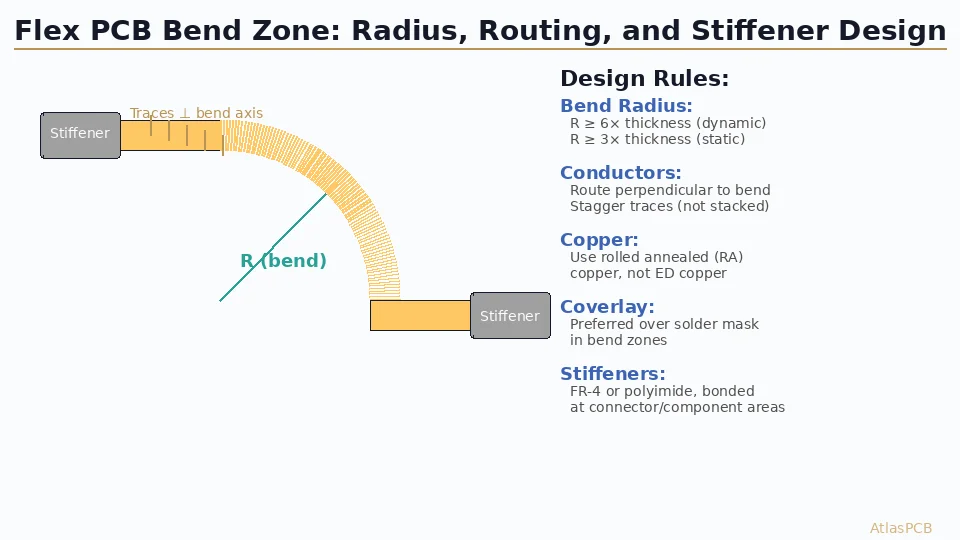
Critical Design Rules for Stiffener Transitions
The transition zone between the stiffened area and the flex bend zone is the highest-stress region in the entire assembly. Design rules for this zone:
Stiffener edge placement — The stiffener edge must be located at least 1.5 mm from the beginning of the bend zone. This creates a gradual stiffness transition rather than an abrupt change that would concentrate stress.
Tapered stiffener edges — Where possible, taper the stiffener thickness at the transition edge, reducing stress concentration by a factor of 2–3× compared to a square edge.
No copper features at the transition — Avoid vias, pads, and trace direction changes within 1.0 mm of the stiffener edge. Copper features at the transition create localized stress risers.
Symmetric stiffener application — For double-sided flex in dynamic applications, apply stiffeners symmetrically on both sides to maintain a neutral bend axis. Asymmetric stiffener placement shifts the neutral axis, increasing strain on the non-stiffened side.
Adhesive selection for stiffener bonding — Use pressure-sensitive adhesive (PSA) or thermal-cure epoxy rated for the operating temperature range. For dynamic applications, PSA provides better shock absorption at the stiffener transition than rigid epoxy bonds.
IPC-2223 Requirements for Dynamic Flex
IPC-2223 (Sectional Design Standard for Flexible Printed Boards) is the primary industry standard governing flex circuit design. Key requirements relevant to dynamic flex:
Conductor Design in Bend Zones
- Conductor routing: All conductors in the bend zone must be perpendicular to the bend axis. Diagonal routing increases the effective stress on conductors during bending.
- Uniform conductor distribution: Space conductors evenly across the bend zone width to distribute strain uniformly. Bunched conductors create local thickness variations and stress concentrations.
- I-beam avoidance: On 2-layer flex, stagger conductors between layers rather than placing them directly above/below each other. Aligned conductors create an I-beam effect that increases bending stiffness and strain.
- No plated through-holes in bend zones: PTH barrels are rigid structures that crack under repeated flexing. All vias and PTHs must be located in stiffened areas outside the bend zone.
- Conductor width: Use the widest conductors that routing density allows. Wider conductors have more cross-sectional area to distribute stress and resist fatigue cracking.
- No sharp corners: Use curved (arc) traces in the bend zone — minimum radius of 0.5 mm for direction changes. Sharp corners create stress concentrations that accelerate fatigue.
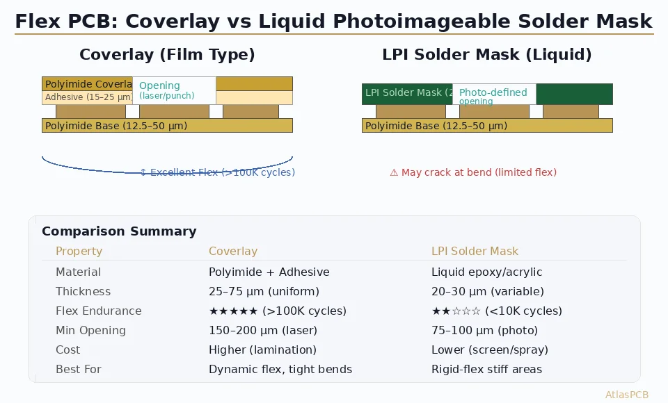
Coverlay Requirements
- Coverlay material: Polyimide coverlay is required in dynamic bend zones. Solder mask (liquid photoimageable) is not suitable — it cracks under repeated flexing.
- Coverlay thickness: Match coverlay thickness on both sides of the flex to maintain a symmetric cross-section and centered neutral axis.
- Coverlay adhesive: For dynamic flex, use low-flow or no-flow adhesive systems to prevent adhesive squeeze-out into the bend zone, which would increase local thickness.
Documentation Requirements
IPC-2223 requires the following to be documented on the fabrication drawing for dynamic flex:
- Minimum bend radius (with indication of static or dynamic)
- Number of flex cycles required
- Operating temperature range during flexing
- Bend zone locations and dimensions
- Copper type specification (RA required for dynamic)
- Stiffener locations, materials, and attachment method
Fatigue Life Testing: MIT Fold Endurance
The MIT Fold Endurance Test
The MIT fold endurance test (per ASTM D2176 or JIS P 8115) is the standard method for evaluating the flex fatigue life of thin materials. A strip of material is clamped in a spring-loaded jaw and folded back and forth through a defined angle (typically 135° in each direction) at a controlled speed (175 double folds per minute).
The test continues until the sample fractures (for bare materials) or until electrical continuity is lost (for flex circuits with conductors). The number of double folds to failure is the fold endurance value.
Typical Fold Endurance Values
| Material / Construction | Fold Endurance (double folds) |
|---|---|
| ED copper, 1 oz, with acrylic adhesive | 200–800 |
| ED copper, ½ oz, with acrylic adhesive | 1,000–3,000 |
| RA copper, ½ oz, with acrylic adhesive | 15,000–50,000 |
| RA copper, ½ oz, adhesiveless | 80,000–200,000 |
| RA copper, ¼ oz, adhesiveless | 200,000–500,000+ |
These numbers illustrate the dramatic impact of copper type and construction on fatigue life:
- Switching from ED to RA copper: 10–50× improvement
- Switching from adhesive-based to adhesiveless: 3–5× improvement
- Reducing copper from ½ oz to ¼ oz: 2–3× improvement
Full Assembly Fatigue Testing
MIT fold endurance tests raw material capability, but actual flex circuit reliability must be validated on the full assembly including coverlay, stiffeners, and conductors. The recommended approach:
Mechanical cycling test — Mount the flex assembly in a fixture that replicates the actual bend radius, bend angle, and bending speed of the application. Cycle continuously while monitoring electrical continuity of daisy-chain test patterns.
Test conditions:
- Bend radius: Application minimum (plus a margin test at 80% of minimum)
- Bend angle: Application maximum
- Cycle rate: 30–60 cycles/minute (representative of typical applications)
- Temperature: Room temperature, and at maximum operating temperature
- Sample size: Minimum 10 samples per condition (per IPC-TM-650 2.4.3)
Pass criteria:
- No continuity failures at 3× the specified cycle life
- No resistance increase > 10% at 1× the specified cycle life
- Visual inspection: No visible cracks, delamination, or coverlay separation
Real-World Applications
Laptop Hinge Connections
Challenge: Connect the display panel to the motherboard through a hinge that opens and closes 20,000+ times over the product’s life. The flex must navigate a tight bend radius (typically 2–4 mm) through a restricted hinge channel.
Design approach:
- Single-layer flex with RA copper, ¼ oz (9 µm)
- Adhesiveless polyimide base (12.5 µm)
- Thin coverlay (12.5 µm polyimide, adhesiveless or with 12.5 µm adhesive)
- Total thickness: ~47–60 µm
- Bend radius: 2.5 mm minimum (>40× thickness)
- Conductor routing: Perpendicular to hinge axis, evenly distributed
- Stiffeners: FR-4, 0.3 mm, at connector attachment areas on both ends
Result: Surface strain at 2.5 mm radius ≈ 0.060/5.0 ≈ 1.2% — conservatively within the fatigue limit for RA copper at 20,000 cycles.
Robotic Arm Cable Assemblies
Challenge: Multi-axis industrial robots require flex cables that traverse 2–6 articulation points, each undergoing continuous motion with millions of cycles over the robot’s service life. Total cable length may be 1–3 meters with multiple bend zones.
Design approach:
- 2-layer flex with RA copper, ½ oz (18 µm)
- Adhesiveless construction throughout
- Total thickness in bend zones: ~80 µm
- Bend radius: 5 mm minimum (>60× thickness) for high-cycle joints
- Staggered conductors (no I-beam stacking)
- Polyimide stiffeners at connectors, stainless steel stiffeners at mounting brackets
- Strain relief at all stiffener transitions
- Spiral or S-curve routing through articulation points to distribute strain
Cycle life target: 10 million cycles — validated through accelerated testing at 80% of minimum bend radius.
Inkjet Printer Head Cables
Challenge: The flex cable connecting the printer head carriage to the main board must flex continuously as the carriage traverses back and forth across the print width — potentially millions of cycles at moderate speed.
Design approach:
- Single-layer flex, RA copper, ⅓ oz (12 µm) for signal lines
- Adhesiveless polyimide, 25 µm base
- Coverlay: 12.5 µm polyimide (adhesiveless)
- Total thickness: ~50 µm
- Bend radius: 4 mm (80× thickness) in the cable chain guide
- U-shaped cable loop that translates with the carriage, maintaining constant bend radius
- Conductors routed in the neutral axis where possible by using symmetric coverlay
- Shielding layer (if needed for EMI): Thin silver ink printed layer rather than copper foil to minimize thickness
Cycle life target: 5+ million cycles, validated by fixture testing with electrical continuity monitoring.
Design Checklist for Dynamic Flex
- ✅ Specify RA copper — Never use ED copper in dynamic bend zones
- ✅ Use adhesiveless construction — Minimize total thickness and improve CTE matching
- ✅ Calculate minimum bend radius — 12× total thickness as starting point; increase for high-cycle applications
- ✅ Route conductors perpendicular to the bend axis — No diagonal routing in bend zones
- ✅ Stagger conductors on 2-layer flex — Avoid I-beam stacking
- ✅ No vias, pads, or components in bend zones — All rigid features in stiffened areas only
- ✅ Use polyimide coverlay, not solder mask — In all bend zones
- ✅ Maintain 1.5 mm minimum clearance from stiffener edges to bend zone start
- ✅ Specify stiffener materials and transitions — Include taper requirements if applicable
- ✅ Document bend parameters on the fab drawing — Radius, cycles, temperature, per IPC-2223
- ✅ Validate with fatigue testing — MIT fold endurance on materials, full assembly cycling on prototypes
Conclusion
Dynamic flex PCB design requires a disciplined approach that spans material science, mechanical engineering, and manufacturing process understanding. The interplay between copper type (RA vs. ED), construction method (adhesiveless vs. adhesive-based), geometry (thickness, bend radius, conductor routing), and operating conditions (cycle count, temperature, bend angle) determines whether a flex circuit will survive for the life of the product or fail prematurely.
By following the IPC-2223 requirements, selecting appropriate materials, calculating bend radius from first principles, and validating designs through rigorous fatigue testing, engineers can design dynamic flex circuits that reliably endure millions of bend cycles. The investment in proper design and testing pays dividends in product reliability and customer satisfaction.
For expert flex and rigid-flex PCB fabrication with advanced material capabilities, visit Atlas PCB to discuss your dynamic flex design requirements with our engineering team. Our HDI PCB services include fine-pitch flex and rigid-flex manufacturing with adhesiveless constructions.
Further Reading
- [PCB Rigid-Flex Bend Zone Reliability: Design Rules, Material Selection & Lifecycle Testing]/blog/pcb-rigid-flex-bend-zone-reliability/)
- [PCB Design for GaN and SiC Power Devices: Thermal Management, Layout Rules, and Material Selection]/blog/pcb-design-gan-sic-power-devices-thermal-layout/)
- [PCB Panelization and Array Design: V-Score vs Tab Routing, DFM Rules, and Cost Optimization]/blog/pcb-panelization-v-score-tab-routing-dfm-cost-optimization/)
- [mmWave PCB Material Selection: Rogers vs Megtron vs LCP for 5G and 6G Applications]/blog/mmwave-pcb-material-selection-rogers-megtron-lcp-5g-6g/)
- [Rogers PCB Fabrication: Material Sourcing, Lead Times & Quality Control]/blog/rogers-pcb-fabrication/)
- Our Manufacturing Capabilities
About AtlasPCB — We specialize in complex PCB manufacturing for HDI, RF, and high-reliability applications. Explore our rigid-flex PCB manufacturing . Every order includes free engineering review. Get your quote.
Reviewed by AtlasPCB Engineering Team — IPC-certified manufacturing specialists with 15+ years of production experience in HDI, RF, and high-reliability PCB fabrication. Content based on factory floor data and real customer design reviews.
- flex PCB
- dynamic flex
- bend radius
- polyimide
- reliability testing