· AtlasPCB Engineering · Engineering · 9 min read
AI-Powered DFM Checking for PCB Design: How Machine Learning Replaces Rule-Based Verification
How AI and machine learning are transforming PCB design-for-manufacturing checks — from static rule engines to intelligent systems that learn defect patterns, predict yield issues, and auto-suggest design fixes.
The Limitations of Rule-Based DFM
For decades, PCB design-for-manufacturing verification has relied on static rule engines. These systems check designs against predetermined geometric constraints: minimum trace width, minimum spacing, annular ring diameter, drill-to-copper clearance, and similar parametric rules. They work — but they have fundamental limitations that become increasingly problematic as designs grow more complex.
What rule-based DFM catches well:
- Explicit geometric violations (trace too narrow, spacing too close)
- Missing features (no thermal relief, no teardrops)
- Dimensional out-of-spec conditions
What rule-based DFM misses:
- Context-dependent issues (acid traps that only matter in certain orientations)
- Cumulative effects (individually-legal features that collectively create yield risk)
- Novel violation patterns (anything not explicitly programmed)
- Manufacturing-specific issues (problems unique to a specific process capability)
A May 2026 article by CrossGen AI published in I-Connect007 captures the core challenge: “The first hard truth about AI in PCB fabrication is that you can buy software, but you cannot buy capability.” This insight applies directly to DFM — buying rules doesn’t create manufacturing intelligence.
How Machine Learning Transforms DFM Checking
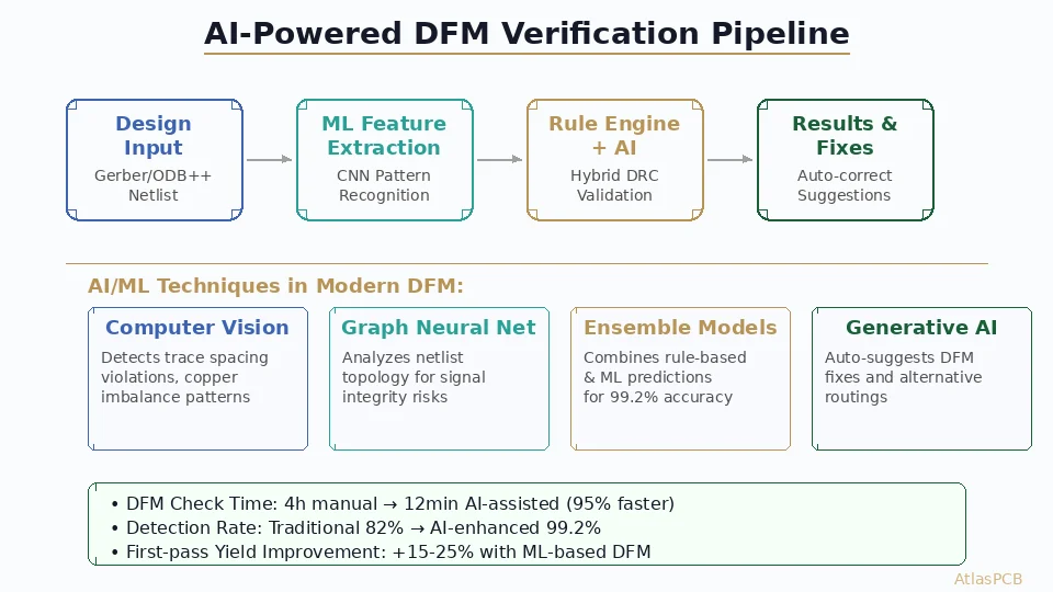
AI-powered DFM represents a paradigm shift from prescriptive rules to learned intelligence. Instead of encoding human knowledge as if/then rules, ML models learn what constitutes a manufacturing risk directly from data — specifically, from thousands of designs paired with their manufacturing outcomes.
Training approach
- Data collection: Gather historical design files (Gerber/ODB++) paired with manufacturing results (yield data, defect reports, rework records)
- Labeling: Annotate specific design features that caused specific manufacturing issues
- Feature extraction: Convert PCB geometry into numerical features the model can process
- Model training: Train on labeled data to learn the relationship between design patterns and manufacturing outcomes
- Validation: Test on held-out data to verify generalization beyond training examples
Model architectures in use
Convolutional Neural Networks (CNNs): Analyze local pattern images for defect-prone geometries. Excels at spatial pattern recognition — acid traps, copper imbalance regions, thermal stress concentrators.
Graph Neural Networks (GNNs): Represent PCB connectivity as a graph and analyze topological relationships. Particularly effective for signal integrity violation prediction and net-level analysis.
Ensemble methods (Random Forest, Gradient Boosting): Combine hundreds of engineered features (area ratios, spacing distributions, layer statistics) for yield prediction at the panel level.
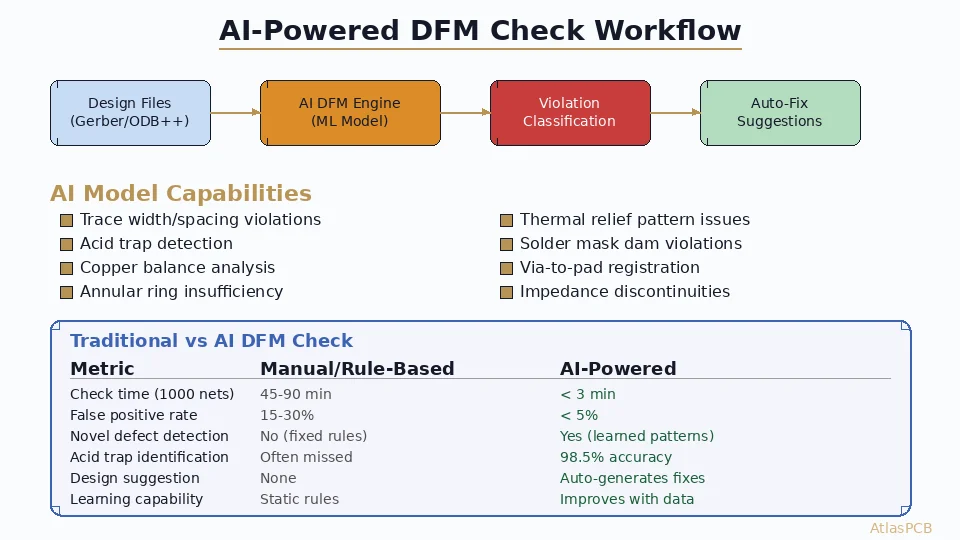
Real-World AI DFM Capabilities
Modern AI DFM systems demonstrated in 2026 can detect:
Acid trap identification (98.5% accuracy)
Acid traps — acute-angle copper features where etchant pools during manufacturing — are notoriously difficult for rule-based systems because whether an angle creates a problem depends on copper thickness, etch chemistry, and surrounding feature density. AI models trained on etch defect data learn the actual risk boundaries.
Copper balance analysis
Rather than simply calculating copper percentages per layer, AI analyzes the spatial distribution of copper density and predicts warpage risk, etch uniformity issues, and plating thickness variation patterns. This catches problems that pass simple “average copper %” rules but fail in production.
Thermal relief optimization
AI identifies pad/plane connections where standard thermal relief patterns will create insufficient heat transfer for reliable soldering — or where overly aggressive thermal connections will cause tombstoning during reflow. Context (component type, pad size, surrounding copper) matters more than fixed rules.
Impedance discontinuity detection
ML models trained on TDR measurement data can predict impedance violations from layout geometry alone — identifying issues that traditional 2D field solvers miss because they don’t account for manufacturing-induced variations in trace width, dielectric thickness, and copper roughness.
Solder mask dam viability
AI predicts whether a solder mask dam will survive development and processing based on dam width, surrounding pad geometry, and board complexity — going beyond simple minimum-width rules to account for manufacturing context.

Free AI-Enhanced DFM Review
Upload your design for comprehensive DFM analysis combining automated rule checks with manufacturing intelligence from thousands of production runs.
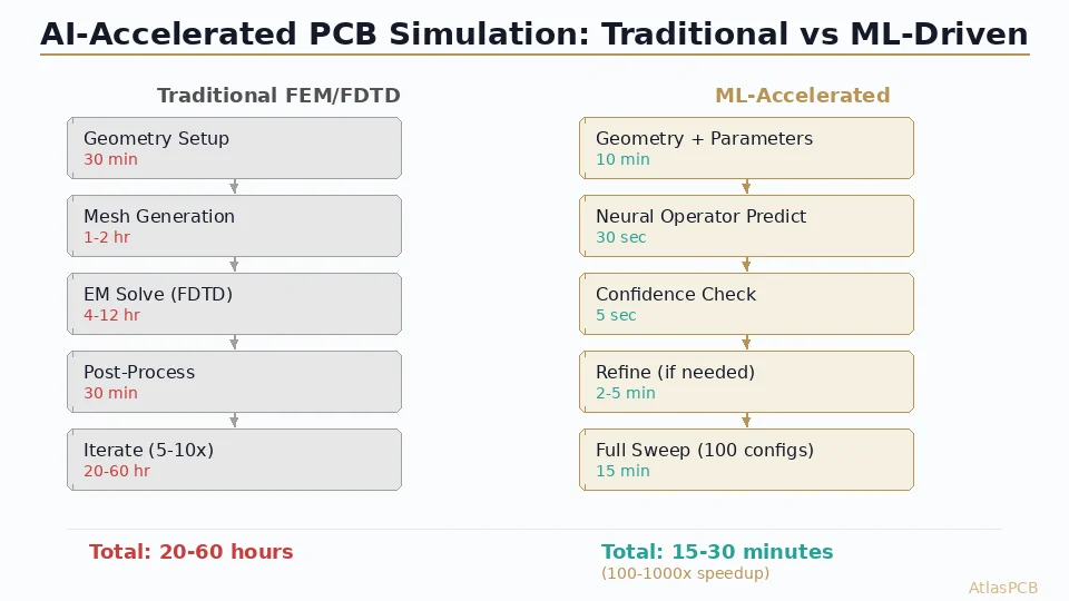
Submit Design for ReviewPerformance Benchmarks: AI vs. Rule-Based DFM
Based on published benchmarks and industry reports from 2025-2026:
| Metric | Rule-Based DFM | AI-Powered DFM |
|---|---|---|
| Check time (1,000-net design) | 45–90 minutes | < 3 minutes |
| False positive rate | 15–30% | < 5% |
| Novel defect detection | No (requires rule update) | Yes (learned patterns) |
| Acid trap identification | ~60% (simple angle check) | 98.5% |
| Yield prediction accuracy | N/A | 85–92% |
| Auto-fix suggestions | None | Generates alternatives |
| Continuous learning | No (manual rule updates) | Yes (improves with data) |
| Setup per new fab | Weeks (rule customization) | Days (model fine-tuning) |
The 10–30× speed improvement alone justifies investigation, but the real value is in catching issues that rules systematically miss — the violations that become yield loss discovered only during production.
Practical Implementation for PCB Fabricators
CrossGen AI’s approach (as described in their I-Connect007 series) emphasizes practical adoption:
Phase 1: Augmentation (months 1-3)
- Run AI DFM in parallel with existing rule-based checks
- Compare outputs to identify where AI catches issues rules miss
- Build confidence through validated catches
- No workflow disruption — AI is advisory only
Phase 2: Integration (months 3-6)
- Route AI-flagged issues to DFM engineers for review
- Begin trusting AI for standard violation categories
- Use AI yield predictions to prioritize engineer review time
- Track AI accuracy metrics continuously
Phase 3: Optimization (months 6+)
- AI handles routine DFM autonomously
- Engineers focus on novel designs and edge cases
- AI auto-fix suggestions presented to designers pre-submission
- Continuous model improvement from production feedback
Data requirements
- Minimum viable dataset: 5,000 labeled design-outcome pairs
- Good performance: 10,000–20,000 examples
- State-of-the-art: 50,000+ with cross-fab generalization
- Critical: balanced representation of pass/fail cases
The Fabricator’s AI Adoption Challenge
The industry faces a capability gap. As CrossGen AI notes: “If the people in your plant do not know how to use AI in real work, then your purchase was more akin to buying a gym membership and never going.”
Key adoption barriers:
- Data fragmentation: Manufacturing data often lives in disconnected systems (CAM, MES, SPC, defect tracking) requiring integration before AI training
- Labeling effort: Converting raw defect data into properly labeled training examples requires domain expertise
- Change management: DFM engineers must evolve from rule authors to model trainers and validators
- Validation rigor: AI systems need rigorous validation before production deployment — especially for high-reliability applications
- Interpretability: Engineers need to understand why AI flags an issue, not just that it flagged it
Impact on PCB Design-Fabrication Interface
AI DFM is reshaping how designers and fabricators interact:
Before AI DFM:
- Designer submits Gerber files
- Fabricator runs rule-based DRC (24-48 hour turnaround)
- Issues communicated back as a PDF list
- Designer fixes and resubmits
- Multiple iterations common (2-4 cycles average)
With AI DFM:
- AI checks design in real-time during layout (EDA plugin)
- Issues flagged with context and suggested fixes as designer works
- By submission time, most issues already resolved
- Fabricator AI confirms compatibility with specific process capabilities
- Submission-to-production time reduces by 40-60%
Connection to AtlasPCB’s Approach
At AtlasPCB, we combine automated DFM checking with engineering expertise built from processing thousands of complex designs. Our review process identifies not just rule violations but manufacturing-risk patterns specific to the technology required — whether that’s HDI with flash copper, high-layer-count builds, or RF/mmWave designs requiring tight impedance control.
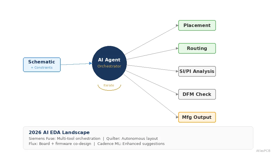
Future: Generative Design Assistance
The next frontier beyond checking is generating. AI systems that:
- Propose optimal stackups given design constraints
- Suggest routing alternatives that improve yield
- Generate copper fill patterns that balance density automatically
- Recommend material selections based on performance/cost trade-offs
This shift from reactive checking to proactive design assistance will fundamentally change the PCB design workflow over the next 3-5 years.
Technical Architecture: Building a PCB DFM AI System
For organizations considering internal AI DFM development, the technical stack typically includes:
Data pipeline
CAM System → Feature Extractor → Label Merger → Training DB
     ↓                                              ↓
[Gerber/ODB++]                              [Yield/Defect Data]
     ↓                                              ↓
Feature Vectors ←─── Spatial Analysis ←─── MES/SPC Integration
Feature engineering for PCB geometry
Key features extracted from PCB designs for ML training:
Local geometry features (per-feature basis):
- Acute angle count and minimum angle value
- Copper density in 1mm, 5mm, and 10mm radius
- Nearest-neighbor trace distance (minimum and average)
- Annular ring minimum value and variance
- Via-to-trace clearance minimum
- Thermal relief connection count and width
Global design features (per-layer/per-board):
- Copper balance percentage (target vs outer layers)
- Layer count and stackup symmetry metric
- Total via count by type (through, blind, buried, microvia)
- Maximum current density estimate (from copper width distribution)
- Impedance structure count and target distribution
Process-aware features:
- Etch factor prediction based on copper weight and trace width
- Registration tolerance impact based on drill-to-copper metrics
- Solder mask registration impact on dam viability
- Lamination bow/twist risk from copper distribution asymmetry
Model deployment architecture
Production AI DFM systems typically deploy as:
- EDA plugin (real-time): Lightweight model running within Altium/KiCad/Allegro for immediate designer feedback
- Cloud inference API (submission-time): Full model with all features for comprehensive analysis
- Batch processing (daily): Retrospective analysis of production outcomes for model improvement
- Edge deployment (on-premise): For facilities with data sovereignty requirements
Training infrastructure
- GPU cluster: 4–8× NVIDIA A100 for model training (or cloud equivalent)
- Storage: 10–50 TB for design file archive with metadata
- MLOps: Model versioning, A/B testing, drift detection
- Annotation tools: Custom GUI for DFM engineer labeling workflow
Case Studies: AI DFM in Production
Case 1: Acid trap reduction at scale
A major HDI fabricator deployed CNN-based acid trap detection on all incoming customer designs. Results after 12 months:
- Acid trap escapes reduced from 2.3% to 0.1% of panels
- Customer design iterations reduced by 40% (issues caught pre-production)
- Annual yield improvement worth approximately $180K in recovered scrap
Case 2: Yield prediction for new designs
Ensemble model trained on 25,000 design-yield pairs predicts first-pass yield within ±5% accuracy for 87% of new designs. This enables:
- Accurate quoting (price reflects actual expected yield)
- Proactive process optimization (known-difficult areas get extra attention)
- Customer communication (data-driven DFM recommendations)
Case 3: Automated copper balance optimization
Generative AI model suggests copper thieving patterns that achieve target density balance while respecting keep-out zones and electrical constraints. Processing time: 30 seconds vs. 2 hours for manual CAM operator.
Ethical Considerations and Limitations
AI DFM systems must be deployed responsibly:
- Intellectual property: Customer designs used for training must have proper data usage agreements
- Bias in training data: Models trained predominantly on consumer electronics may perform poorly on military/aerospace designs
- Transparency: Engineers must understand model confidence levels and limitations
- Failure modes: Clear fallback procedures when AI confidence is low
- Continuous validation: Regular testing against known-good and known-bad designs prevents model degradation
Further Reading
- AOI and SPI Inspection for PCB Assembly Quality
- PCB Etch Compensation Design
- Common PCB Defects and Prevention
- IPC-2581 Digital Twin PCB Data Exchange
Want manufacturing-intelligent DFM review? AtlasPCB’s engineering team combines automated analysis with deep process expertise. Submit your design for review — we’ll identify yield risks that standard rule checks miss.
About AtlasPCB — We specialize in complex PCB manufacturing for HDI, RF, and high-reliability applications. Explore our free engineering DFM review . Every order includes free engineering review. Get your quote.
Reviewed by AtlasPCB Engineering Team — IPC-certified manufacturing specialists with 15+ years of production experience in HDI, RF, and high-reliability PCB fabrication. Content based on factory floor data and real customer design reviews.
- AI DFM
- machine learning
- PCB design
- design for manufacturing
- automated verification
- AI PCB
- defect prediction
- manufacturing intelligence