· AtlasPCB Engineering · Engineering · 10 min read
AOI and SPI Inspection in PCB Assembly: Automated Optical Inspection Technology for Zero-Defect Manufacturing
Complete guide to AOI and SPI inspection systems in PCB assembly. Covers solder paste inspection principles, automated optical inspection algorithms, 3D measurement technology, defect classification, programming strategies, and integration with Industry 4.0 traceability systems.

Introduction: The Economics of Inline Inspection
In modern PCB assembly, a single undetected defect that reaches the customer costs 10-100× more to resolve than catching it on the production line. An MLCC capacitor worth $0.003 that causes a field failure may generate $500-5,000 in warranty repair, logistics, and reputation costs. This economic reality drives the adoption of automated inspection systems at every critical process step.
SPI (Solder Paste Inspection) and AOI (Automated Optical Inspection) form the quality backbone of SMT assembly lines. Together, they provide closed-loop process control that catches defects at their source, enables immediate corrective action, and generates the data needed for continuous process improvement.
This guide covers the technology, implementation, and optimization of both inspection systems—from the physics of measurement to the practical programming strategies that differentiate zero-defect manufacturers from those drowning in false calls and escaped defects.
Solder Paste Inspection (SPI): Catching Defects at the Source
Why SPI Is the Highest-ROI Inspection
Research consistently shows that 60-70% of all SMT assembly defects originate from solder paste printing. Poor paste deposits lead directly to:
- Insufficient solder: Cold joints, head-in-pillow on BGAs (see [reflow profile optimization]/blog/reflow-soldering-profile-optimization-lead-free-pcb-assembly/))
- Excess solder: Bridging between adjacent pads
- Misaligned paste: Tombstoning, mid-chip solder balls
- Slumped paste: Shorts on fine-pitch components
- Missing paste: Open circuits, non-wetting
By inspecting 100% of paste deposits immediately after printing, SPI enables:
- Detection before component placement adds value
- Board rejection before expensive ICs are mounted
- Immediate feedback for printer parameter adjustment
- Statistical process control on printing quality
SPI Measurement Technology
Modern SPI systems use 3D measurement to characterize every paste deposit:
Phase-Shift Profilometry
The dominant SPI technology projects structured light patterns (sinusoidal gratings) onto the paste surface from multiple angles. Phase differences between projected and reflected patterns encode height information:
- Resolution: 10-15μm lateral, 1-2μm vertical
- Speed: 20-40 cm²/second
- Accuracy: ±2μm height, ±1% volume
- Limitation: Struggles with highly reflective surfaces (gold pads)
Laser Triangulation
A laser line scans across the board surface while a camera at an angle detects displacement:
- Resolution: 5-10μm lateral, 0.5-1μm vertical
- Speed: Slower (10-15 cm²/second)
- Accuracy: ±1μm height
- Advantage: Less affected by surface reflectivity
SPI Measurement Parameters
For each paste deposit, SPI measures and evaluates:
| Parameter | Definition | Typical Tolerance | Significance |
|---|---|---|---|
| Volume | 3D integrated paste amount | ±50% nominal | Primary quality predictor |
| Height | Maximum or average paste height | ±30% stencil thickness | Indicates squeegee pressure |
| Area | 2D footprint coverage | ±50% pad area | Indicates aperture fill/release |
| Offset X/Y | Centroid deviation from pad center | ±25% pad width | Predicts tombstoning |
| Shape | Circularity/rectangularity | Application-specific | Indicates print wear |
| Bridge | Paste connecting adjacent pads | Zero tolerance | Direct short circuit |
SPI Process Windows by Component Type
Different components require different paste specifications:
Fine-pitch BGA (0.4mm pitch):
- Volume: 8,000-14,000 mil³ per pad
- Height tolerance: ±15μm
- Offset: <50μm from pad center
- Bridge detection: mandatory between all adjacent pads
Standard chip components (0402-0805):
- Volume: 3,000-12,000 mil³ (size-dependent)
- Height tolerance: ±25μm
- Volume ratio between pads: <1.5:1 (tombstone prevention)
QFN exposed pad:
- Volume: Application-specific (thermal vs. electrical)
- Patterned print: Multiple deposits within pad area
- Total volume: Typically 50-60% pad area × stencil thickness
SPI-to-Printer Closed Loop
Advanced SPI systems communicate directly with the printer for automatic correction:
- SPI detects trending offset → Printer adjusts alignment
- SPI detects volume decrease → Printer triggers stencil cleaning
- SPI detects bridging increase → Printer reduces squeegee pressure or speed
- SPI detects height variation → Printer adjusts separation speed
This closed-loop operation reduces operator intervention and maintains printing quality during extended production runs where paste rheology changes and stencil apertures accumulate residue.
Automated Optical Inspection (AOI): Post-Placement and Post-Reflow
AOI System Architecture
A modern 3D AOI system combines multiple imaging technologies:
Camera system:
- High-resolution area cameras (5-29 megapixel)
- Telecentric lenses for distortion-free imaging
- Multiple cameras at different angles (typically 1 vertical + 4 angled at 35-55°)
Illumination:
- Multi-spectral LED arrays (red, green, blue, white, UV, IR)
- Ring lights at various angles (0°, 30°, 60°, 90°)
- Programmable intensity for different component/surface combinations
- Structured light projector for 3D measurement
3D measurement:
- Phase-shift profilometry (structured light at 4-8 patterns)
- Laser triangulation for specific features
- Stereo vision from angled cameras
- Resolution: 5-15μm lateral, 1-5μm vertical
Inspection Capabilities by Process Stage
Post-Placement AOI
Inspects after component placement, before reflow:
- Component presence/absence
- Component value verification (resistor color bands, capacitor markings)
- Polarity verification (ICs, diodes, tantalum capacitors)
- Placement accuracy (X, Y, θ offset from nominal)
- Coplanarity of lead-frame components
- Flipped components
- Wrong components (size verification)
Post-Reflow AOI
Inspects after solder joints have formed:
- All post-placement checks plus:
- Solder joint quality (insufficient, excess, bridging)
- Tombstoning (mid-process failure) — see our [solder paste stencil design guide]/blog/pcb-solder-paste-stencil-design/)
- Solder balls (loose conductive particles)
- Lifted leads on gull-wing packages
- Cold joints (grainy, non-wetting appearance)
- Component shift during reflow
- Damaged components (cracked ceramic, burnt marks)
- Missing components (fallen off during reflow)
AOI Algorithm Categories
Modern AOI systems use multiple algorithm types in combination:
Pattern Matching (Template-Based)
- Compares captured image region against stored reference
- Fast and robust for component presence/polarity
- Requires golden board programming
- Sensitive to lighting variation
Feature Extraction
- Identifies geometric features (edges, corners, circles)
- Measures dimensions and positions
- Less dependent on exact appearance
- Better for components with variable markings
Color/Grayscale Analysis
- Evaluates color distribution on solder joints
- Bright regions indicate good wetting; dark regions suggest defects
- Ring illumination creates characteristic reflection patterns on convex (good) vs. concave (bad) joints
- Effective for through-hole and large SMT joints
3D Height Analysis
- Measures solder fillet height profile
- Detects insufficient solder (flat or concave profile)
- Identifies bridging (height continuity between pads)
- Evaluates lifted leads (gap between lead and pad)
- Most reliable method for fine-pitch (≤0.5mm) leads
AI/Deep Learning
- Neural networks trained on defect image databases
- Excels at classifying ambiguous borderline cases
- Reduces false calls by 30-50% on challenging features
- Requires extensive training data (>10,000 labeled images)
- Used for solder joint classification, component damage detection
Quality-First PCB Assembly with 100% Inspection
AtlasPCB's assembly lines feature inline SPI, 3D AOI, and X-ray inspection ensuring zero-defect quality for your critical electronics products.
Get Your PCBA Quote →AOI Programming Best Practices
Golden Board Approach
The most effective AOI programming methodology:
- Build 5-10 boards through normal production
- Inspect manually to confirm they are defect-free
- Program AOI using these boards as reference
- Statistical baseline: System learns normal variation from multiple samples
- Set thresholds based on measured distribution + safety margin
Threshold Optimization Strategy
Initial setup (conservative):
- Set all thresholds at ±3 sigma from golden board measurements
- Accept higher false call rate initially
- Run 100-500 boards collecting data
Optimization phase:
- Analyze Pareto chart of false calls by component/feature
- Widen thresholds on high-false-call features (verify no real defects escaped)
- Tighten thresholds on features where defects were found
- Target: <0.5% false call rate, <20 DPM escape rate
Ongoing maintenance:
- Weekly review of false call Pareto
- Monthly verification of escape rate (sample X-ray or destructive analysis)
- Re-optimize after paste/component/process changes
Component Library Management
Maintain standardized inspection recipes for component packages:
- 0402 chip (generic): Height range, body size, termination color, polarity mark
- BGA 0.8mm pitch: Ball presence pattern, ball diameter range, bridge threshold
- QFP 0.5mm pitch: Lead coplanarity, lead tip position, solder fillet profile
- QFN 0.5mm pitch: Side fillet height (if visible), void area (3D measurement)
Standardized libraries reduce programming time for new products from days to hours.
X-Ray Inspection: Seeing Hidden Joints
For components with hidden solder joints (BGA, QFN, LGA, bottom-terminated), AOI cannot directly evaluate joint quality. X-ray inspection fills this gap:
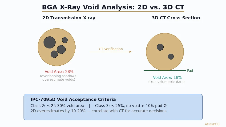
2D X-Ray
- Transmission imaging through the board
- Detects BGA voiding, bridging, missing balls
- Cost-effective for sample inspection
- Limited for multi-layer BGAs (overlapping images)
3D CT (Computed Tomography)
- Reconstructs 3D volume from multiple angle projections
- Individual layer slicing—examines any depth
- Definitive void measurement, crack detection
- Slower (1-5 minutes per board section)
- Used for failure analysis and process development
When X-Ray Is Mandatory
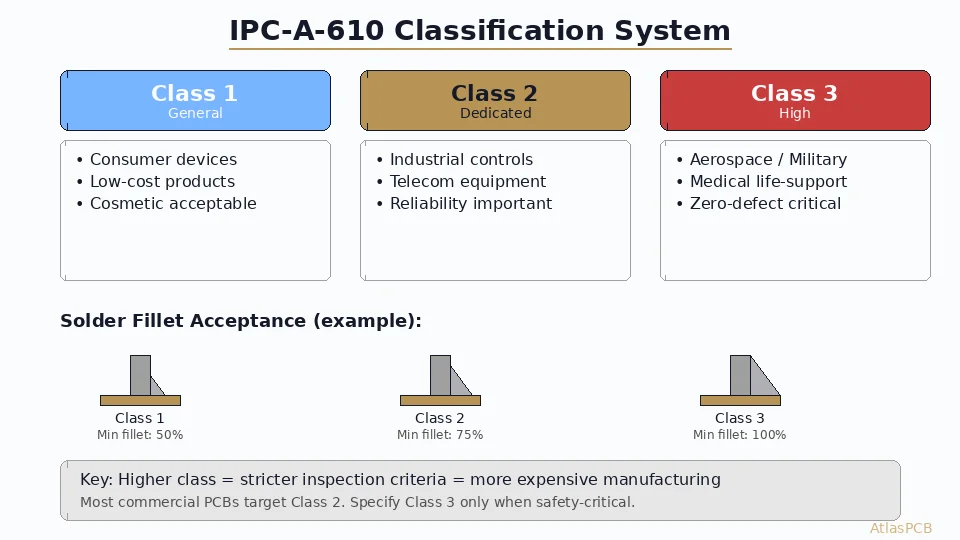
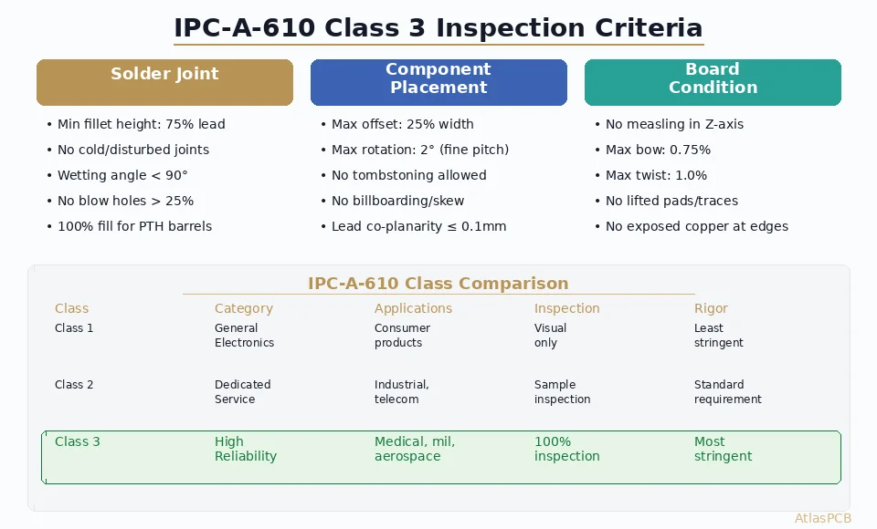
- BGA inspection (all classes per [IPC-A-610]/blog/ipc-a-600-class-2-vs-class-3-pcb-acceptability/))
- QFN thermal pad voiding evaluation
- LGA/flip-chip joint quality verification
- Lead-free joint crack analysis
- Failure analysis of field returns
Industry 4.0 Integration: From Inspection to Intelligence
Traceability Data Flow
Modern inspection systems generate massive data that, properly connected, enables predictive quality:
Printer → SPI → Placer → Post-place AOI → Reflow → Post-reflow AOI → X-ray → Test
   |         |       |           |             |            |             |       |
   v         v       v           v             v            v             v       v
                    Unified Manufacturing Execution System (MES)
                              ↓
                    Statistical Analysis / AI
                              ↓
                    Predictive Process Control
Correlation Analysis
By linking inspection data across process steps:
- SPI volume vs. AOI solder joint: Validates SPI limits against actual defects
- Placement offset vs. post-reflow position: Quantifies self-centering during reflow
- SPI bridge warning vs. post-reflow short: Determines which SPI warnings are real risks
- Oven profile data vs. AOI defect clusters: Correlates thermal drift with quality
Machine Learning for Process Prediction
Training models on inspection+process data enables:
- Predicting which boards will fail test based on SPI/AOI measurements
- Identifying process drift before it causes defects
- Optimizing printer/placer/reflow parameters based on inspection feedback
- Reducing inspection time by adapting sensitivity based on process stability
Inspection Economics: Calculating ROI
Cost of a Missed Defect
The cost multiplier at each stage:
| Detection Stage | Relative Cost | Example Cost |
|---|---|---|
| SPI (post-print) | 1× | $0.10 (board rework) |
| Post-placement AOI | 5× | $0.50 (remove/replace component) |
| Post-reflow AOI | 10× | $1.00 (BGA rework) |
| ICT/FCT | 50× | $5.00 (diagnosis + rework) |
| Customer return | 500-5000× | $50-500 (warranty + logistics + reputation) |
SPI ROI Example
Investment: $150,000 (3D SPI system) Line capacity: 200 boards/hour, 16 hours/day Defect rate without SPI: 500 DPM (paste-related) Defect rate with SPI: 50 DPM (90% catch rate) Boards/year: 200 × 16 × 250 = 800,000
Defects prevented: (500-50) × 800,000 / 1,000,000 = 360 boards/year Average rework cost per defect at ICT: $15 Annual savings: 360 × $15 = $5,400 in rework alone Annual savings including field returns prevented: $50,000+ Payback period: <3 years (conservative)
Common SPI/AOI Implementation Mistakes
Mistake 1: Inspecting But Not Acting
Installing inspection equipment without closed-loop response procedures is surveillance without security. Every failed inspection must trigger a defined action:
- SPI fail: Board rejected, printer parameters checked, stencil cleaned if bridge
- AOI fail: Board routed to repair station, defect classified, root cause investigated
- Repeat fails on same feature: Engineering review triggered, not just operator override
Mistake 2: Operator Override Culture
When false calls are high, operators learn to override AOI rejections without careful verification. This creates a culture where real defects also get overridden. Solution: reduce false calls through proper programming rather than accepting them and training operators to dismiss alarms.
Mistake 3: Programming Once, Never Updating
Process variation changes over time—new paste lots, stencil wear, seasonal humidity variation. AOI programs must evolve with the process:
- Monthly threshold review
- Quarterly golden board refresh
- Annual full program re-validation
Mistake 4: Ignoring SPI Data for Process Improvement
SPI generates the most valuable data on the SMT line—it shows exactly where printing is trending before defects occur. Use SPI trends for:
- Stencil life prediction (aperture wear monitoring)
- Paste freshness tracking (volume consistency over time)
- Environmental correlation (humidity vs. paste performance)
- Operator skill assessment (print quality by shift/operator)
Future Trends in PCB Assembly Inspection
AI-Powered Defect Classification
Deep learning is rapidly improving AOI accuracy:
- Self-learning algorithms that improve with production data
- Cross-product transfer learning (lessons from one board improve detection on another)
- Reduced programming time (minutes vs. hours)
- Better handling of component variation (different manufacturers of same part)
Hyperspectral Imaging
Beyond RGB cameras, new systems use hyperspectral imaging to:
- Distinguish solder alloy composition
- Detect contamination invisible to standard cameras
- Identify material defects (wrong component even if same size)
- Evaluate flux residue quality
Inline CT X-Ray
Emerging systems combine conveyor transport with computed tomography:
- Full 3D inspection of hidden joints at line speed
- Eliminates the AOI blind spot for BGA/QFN
- Currently limited to <30 seconds per board (improving rapidly)
- Expected to become standard for automotive/aerospace by 2028
Conclusion: Building a Quality-Centered Inspection Strategy
Effective PCB assembly inspection isn’t about buying the most expensive equipment—it’s about building an integrated quality system where each inspection point serves a defined purpose, data flows between systems, and the organization acts on inspection findings.
Implementation priority:
- SPI first: Highest ROI, catches defects at source
- Post-reflow AOI second: Verifies final product quality
- Post-placement AOI third: Catches placement errors before they become expensive
- X-ray for hidden joints: Sample or 100% depending on criticality
The manufacturers who achieve true zero-defect performance aren’t those with the most inspection machines—they’re those who close the loop between inspection data and process control, turning every detected defect into a process improvement that prevents its recurrence.
AtlasPCB provides full inline inspection on every assembly order—SPI, 3D AOI, and X-ray for BGA/QFN packages. Our quality system ensures your products meet IPC Class 2 or Class 3 standards with full traceability. Get a quote for your next assembly project.
Further Reading
- [Rogers PCB Fabrication: Material Sourcing, Lead Times & Quality Control]/blog/rogers-pcb-fabrication/)
- [PCB Rigid-Flex Bend Zone Reliability: Design Rules, Material Selection & Lifecycle Testing]/blog/pcb-rigid-flex-bend-zone-reliability/)
- [ENEPIG vs ENIG Surface Finish: Complete Comparison for Wire Bonding, Solderability, and Long-Term Reliability]/blog/enepig-vs-enig-surface-finish-wire-bonding/)
- [PCB Surface Finish Comparison: OSP vs HASL vs Immersion Silver vs ENIG for Assembly Reliability]/blog/pcb-surface-finish-osp-hasl-enig-immersion-silver-comparison/)
- [PCB Manufacturer with Engineering Review: Why Human DFM Audit Matters]/blog/pcb-manufacturer-engineering-review/)
- Our Manufacturing Capabilities
About AtlasPCB — We specialize in complex PCB manufacturing for HDI, RF, and high-reliability applications. Explore our PCB assembly services, or get an full PCB manufacturing capabilities . Every order includes free engineering review. Get your quote.
Reviewed by AtlasPCB Engineering Team — IPC-certified manufacturing specialists with 15+ years of production experience in HDI, RF, and high-reliability PCB fabrication. Content based on factory floor data and real customer design reviews.
- AOI
- SPI
- PCB inspection
- quality control
- automated optical inspection
- solder paste inspection
- PCBA
- zero-defect manufacturing