· AtlasPCB Engineering · Engineering · 8 min read
Flash Copper Plating for HDI Microvias: Achieving Uniform Seed Layers in mSAP Process
Technical deep-dive into flash copper plating technology for HDI blind microvias — process parameters, seed layer uniformity, and advantages over electroless copper for mSAP and advanced substrate fabrication.
Introduction: The Critical Role of Seed Layers in HDI
In high-density interconnect PCB fabrication, the seed layer — that first sub-micron coating of copper on via walls and panel surfaces — determines everything that follows. Too thin, and subsequent plating fails to initiate uniformly. Too thick, and fine-line resolution suffers during etch-back. Uneven, and via fill plating develops voids.
Flash copper plating has emerged as the preferred seed layer technology for advanced HDI and modified semi-additive process (mSAP) boards. Originally developed for IC substrate manufacturing where feature sizes demand extraordinary uniformity, flash copper is now migrating into mainstream HDI production for smartphones, AI modules, and high-performance computing applications.
A May 2026 technical feature in I-Connect007’s PCB magazine highlighted innovative flash copper plating chemistry specifically designed for HDI blind microvias, noting that the “continuous push toward higher functionality, miniaturization, and performance in modern electronic devices has intensified the demand for reliable formation of blind microvias.”
What Makes Flash Copper Different
Flash copper plating is fundamentally an electrolytic process — it uses externally applied current to reduce copper ions from solution onto the workpiece. This distinguishes it from electroless copper, which relies on formaldehyde-driven autocatalytic reduction. The key characteristics:
Process parameters
| Parameter | Flash Copper | Electroless Copper |
|---|---|---|
| Deposition mechanism | Electrolytic (current-driven) | Autocatalytic (chemical) |
| Typical thickness | 0.3–0.8 μm | 0.3–1.5 μm |
| Deposition time | 5–10 minutes | 20–30 minutes |
| Current density | 1.5–3.0 ASD | N/A (no current) |
| Bath temperature | 22–28°C | 28–35°C |
| pH | 12.0–13.0 (alkaline) | 12.5–13.5 |
| Formaldehyde | Not required | Required (reducing agent) |
| Palladium catalyst | Not required* | Required |
| Copper purity | >99.9% | >99.5% |
| Grain structure | Columnar, oriented | Amorphous, fine-grained |
*Flash copper requires prior direct metallization (carbon/graphite/polymer) instead of Pd catalyst
Why “flash” and not regular plating?
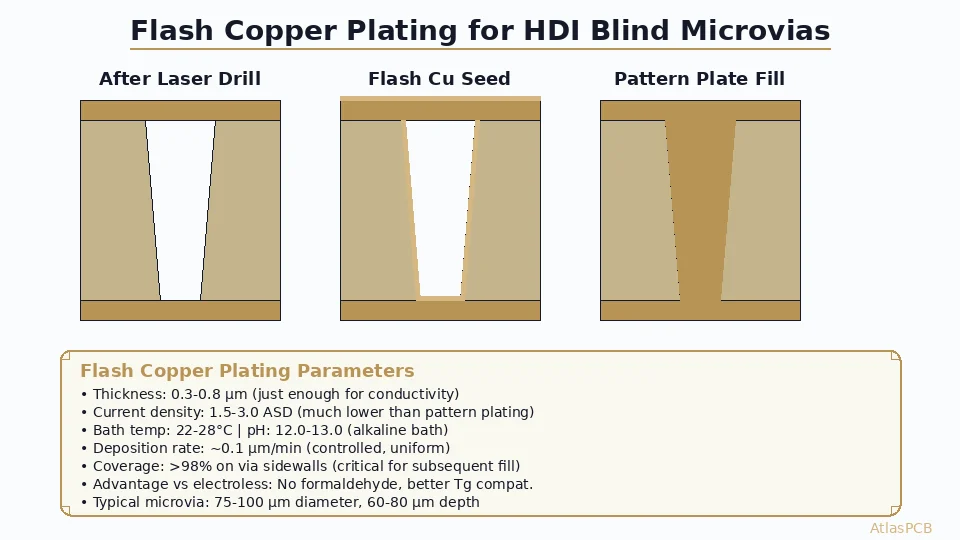
The term “flash” refers to the extremely short plating time and low current density compared to standard pattern or panel plating. Regular DC acid copper plating operates at 2–4 ASD for 40–60 minutes to deposit 20–35 μm. Flash copper operates at 1.5–3.0 ASD for just 5–10 minutes, depositing only 0.3–0.8 μm — enough for conductivity but minimal enough to preserve fine-line resolution.
The mSAP Connection
The modified Semi-Additive Process (mSAP) is the dominant patterning technology for HDI boards with line/space below 30/30 μm. mSAP relies on an ultra-thin copper seed layer that is:
- Applied uniformly across the panel surface and via walls
- Thick enough to support uniform pattern plating
- Thin enough to be removed cleanly during differential etching without excessive line-width reduction
In mSAP, the seed layer thickness directly impacts minimum achievable line width. A 0.5 μm seed requires removing only 0.5 μm from each side during etch-back, allowing 15 μm traces to be patterned with acceptable line-width variation. A 1.5 μm electroless seed requires removing 1.5 μm per side, making the same 15 μm trace significantly more challenging.
This is why flash copper at 0.3–0.5 μm is preferred over electroless copper at 0.8–1.5 μm for mSAP applications.
Flash Copper Bath Chemistry
Modern flash copper baths use alkaline (pyrophosphate or cyanide-free complexed) chemistry rather than the acid sulfate baths used for pattern plating. The alkaline environment provides:
Bath composition (typical)
- Copper content: 3–8 g/L (as Cu²⁺)
- Complexing agent: EDTA, tartrate, or proprietary
- pH: 12.0–13.0 (maintained by NaOH)
- Temperature: 22–28°C
- Brightener/leveler: Proprietary additives for uniformity
Advantages of alkaline flash copper
- Superior throwing power: Alkaline baths deposit more uniformly into via holes compared to acid baths, achieving >95% via sidewall coverage even at aspect ratios of 1.2:1
- Better adhesion to dielectric: Alkaline pH promotes copper nucleation on conditioned dielectric surfaces
- Compatibility with direct metallization: Works directly on carbon/graphite-treated surfaces
- Reduced hydrogen embrittlement: Lower hydrogen evolution at cathode compared to acid baths
Process Integration: From Drill to Pattern Plate
The complete flash copper process sequence in an HDI production line:
Laser Drill → Desmear (plasma/permanganate) → Conditioning →
Direct Metallization (carbon/graphite) → Micro-etch →
Flash Copper Plating → Dry Film Lamination → Pattern Expose →
Develop → Pattern Copper Plate (fill) → Strip → Etch-back
Each step interfaces critically with flash copper:
Before flash copper:
- Desmear quality determines dielectric surface morphology
- Direct metallization provides the initial conductive path
- Micro-etch activates copper surfaces for bonding
After flash copper:
- Dry film must adhere to the thin flash copper surface
- Pattern plating initiates on the flash copper seed
- Etch-back must cleanly remove flash copper between traces
Advanced HDI & mSAP Manufacturing
AtlasPCB manufactures HDI boards with L/S down to 25/25 μm using advanced flash copper and mSAP processes.
Get a Free DFM ReviewAchieving Uniformity: Critical Process Controls
Flash copper uniformity across a 510×610 mm production panel is the primary process challenge. Key control parameters:
Current distribution
- Anode configuration: Soluble copper anodes positioned for uniform current distribution
- Shield/thief design: Edge thieves absorb excess current at panel periphery
- Auxiliary anodes: Additional anodes near panel edges compensate for edge effects
- Current density mapping: Target ±10% uniformity across panel (±15% maximum)
Bath agitation
- Gentle air agitation (not vigorous — risk of seed layer damage)
- Panel oscillation: 15–20 cycles/min, 25–50 mm stroke
- Solution flow rate: 3–5 panel volumes per minute
Monitoring
- Hull cell testing: Daily for deposit quality assessment
- Thickness measurement: XRF or cross-section (every lot)
- Coverage verification: Backlight test for via sidewall continuity
- Bath analytics: Cu²⁺ concentration, pH, additive levels (every 4 hours)
Blind Microvia Fill After Flash Copper
Flash copper provides the seed for subsequent via fill plating. The fill plating process uses specialized “bottom-up” chemistry with:
- Suppressor: Adsorbs on flat surfaces, inhibiting deposition
- Accelerator: Concentrates at via bottom, promoting faster deposition there
- Leveler: Controls top-surface planarity
The result is vias that fill from the bottom up without void formation — critical for stacked microvia reliability in any-layer HDI designs.
Fill plating process sequence
After flash copper establishes the seed layer, the panel enters the DC acid copper fill plating bath:
- Initial nucleation phase (0–5 min): Low current density 0.5–1.0 ASD to establish uniform copper growth on the flash seed
- Bottom-up fill phase (5–30 min): Ramp to 1.5–2.5 ASD with additive-controlled differential deposition
- Leveling phase (30–45 min): Current maintained while leveler additive planarizes the via top
- Overplate phase (if needed): Additional 2–5 μm to ensure flush or slightly domed via surface
Via fill quality criteria (per IPC-6012E)
- Target fill: ≥75% for standard HDI; ≥90% for stacked microvia applications
- Dimple depth: <15 μm for subsequent layer lamination
- Void content: <5% by cross-sectional area (class 3); <10% (class 2)
- Copper cap thickness: Uniform ±20% across panel
Comparison: Flash Copper vs. Electroless Copper vs. Direct Metallization Alone
Understanding the relationship between these technologies:
| Technology | Function | Thickness | Limitations |
|---|---|---|---|
| Direct metallization alone | Makes holes conductive | ~100-200 nm (carbon) | High resistance; slow initial plating |
| Electroless copper | Autocatalytic seed | 0.3–1.5 μm | Formaldehyde, Pd catalyst, slow |
| Flash copper (on direct met.) | Electrolytic seed | 0.3–0.8 μm | Requires prior conductive layer |
| Flash copper (on electroless) | Additional seed | 0.3–0.5 μm | Two-step approach, costly |
The most advanced production flow combines direct metallization + flash copper, eliminating electroless copper entirely from the process chain. This provides:
- Environmental benefits of direct metallization (no formaldehyde, no Pd)
- Superior seed uniformity of electrolytic flash copper
- Optimal thickness control for mSAP fine-line patterning
Failure Modes and Prevention
Skip plating (incomplete coverage)
Symptom: Isolated spots where copper doesn’t plate on via sidewall Root cause: Flash copper too thin in localized areas; direct metallization incomplete Prevention: Verify direct metallization coverage via backlight test; increase flash copper time by 20%; improve agitation uniformity
Nodule formation
Symptom: Rough copper surface with protruding crystallites Root cause: Excessive current density at flash copper step; bath contamination Prevention: Maintain current density below 3.0 ASD; carbon filter bath continuously; monitor organics
Poor adhesion at via knee
Symptom: Copper lifts from dielectric at the junction between top copper and via wall Root cause: Inadequate desmear leaving resin residue; sharp angle concentrates stress Prevention: Optimize desmear parameters; ensure adequate conditioning; consider laser-shaped via profile with gentler taper angle
Thickness non-uniformity (>±30%)
Symptom: Flash copper varies significantly across panel or between via top and bottom Root cause: Current distribution issues; poor anode configuration; inadequate agitation Prevention: Install edge thieves; verify anode-to-cathode distance uniformity; optimize panel oscillation parameters
Economic Considerations
For a facility processing 5,000 panels/month of HDI boards:
Process cost comparison (per panel)
| Cost element | Electroless Cu | Flash Cu + Direct Met. |
|---|---|---|
| Chemistry | $3.20 | $2.10 |
| Palladium | $0.80 | $0.00 |
| Energy | $0.15 | $0.25 |
| Water treatment | $0.40 | $0.15 |
| Labor (process time) | $1.20 | $0.80 |
| Total | $5.75 | $3.30 |
| Monthly savings | — | $12,250 |
Capital investment for conversion: approximately $200K–400K for a single plating line (new flash copper tank, rectifier, controls). Payback at 5,000 panels/month: approximately 24 months.
Quality Metrics for Flash Copper Evaluation
| Metric | Target | Test Method |
|---|---|---|
| Thickness | 0.3–0.8 μm ±20% | XRF, cross-section |
| Coverage (sidewall) | >95% of via depth | Cross-section SEM |
| Adhesion (peel) | >0.4 N/mm | IPC-TM-650, 2.4.8 |
| Surface roughness (Rz) | 0.5–2.0 μm | Profilometer |
| Resistivity | <2.0 μΩ·cm | Four-point probe |
| Void rate (after fill) | <1% by area | X-ray, cross-section |
Future Directions
Flash copper technology continues evolving:
- Thinner deposits: Push toward 0.2–0.3 μm for sub-15 μm L/S in next-gen substrates
- Pulse plating: Periodic reverse pulse improves uniformity in deep vias
- Novel additives: Bio-based leveling agents replacing traditional toxic suppressors
- In-line monitoring: Real-time thickness measurement using eddy current sensors
- Integration with SAP: Moving beyond mSAP to full semi-additive process for <10 μm features
Further Reading
- HDI Microvia: Stacked vs Staggered Reliability
- PCB Copper Plating: Electroless vs Electrolytic for HDI Vias
- VIPPO Via-in-Pad Plated Over Design and Manufacturing
- PCB Laser Drilling: CO2 vs UV Microvia Quality
Designing with HDI microvias? AtlasPCB’s engineering team can review your stackup and recommend optimal plating parameters for your design requirements. Contact us for a free DFM review.
About AtlasPCB — We specialize in complex PCB manufacturing for HDI, RF, and high-reliability applications. Explore our HDI PCB manufacturing capabilities . Every order includes free engineering review. Get your quote.
Reviewed by AtlasPCB Engineering Team — IPC-certified manufacturing specialists with 15+ years of production experience in HDI, RF, and high-reliability PCB fabrication. Content based on factory floor data and real customer design reviews.
- flash copper plating
- HDI
- microvia
- mSAP
- seed layer
- copper plating
- blind via
- IC substrate
- advanced packaging