· AtlasPCB Engineering · Engineering · 8 min read
PCB Laser Drilling: CO₂ vs UV Parameters for Optimal Microvia Quality
Compare CO₂ and UV laser drilling for PCB microvias. Detailed parameter guides for pulse energy, repetition rate, focus control, and quality metrics including taper angle, smear, and copper damage.

Why Laser Drilling Defines HDI Capability
Every HDI PCB begins with a hole — specifically, a microvia connecting adjacent layers that enables the routing density modern ICs demand. The quality of that microvia determines everything downstream: plating reliability, via resistance, thermal cycling endurance, and ultimately product lifetime.
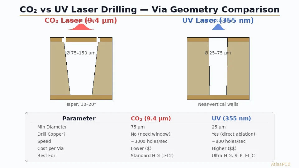
Two laser technologies dominate PCB microvia drilling: CO₂ lasers operating at 9.4-10.6 μm wavelength, and UV solid-state lasers (typically Nd:YAG third harmonic at 355 nm). Each has fundamentally different interaction physics with PCB materials, resulting in different via geometries, throughput rates, and cost profiles.
Understanding when to specify each technology — and what process parameters to control — separates robust HDI designs from those that suffer microvia reliability failures in the field. This guide provides the engineering detail needed to make informed decisions and communicate effectively with your PCB fabricator.
Laser-Material Interaction Physics
CO₂ Laser (9.4–10.6 μm)
The CO₂ laser’s infrared wavelength interacts with PCB materials through thermal absorption:
Dielectric (FR-4 resin + glass):
- Strong absorption by organic resin — rapid thermal decomposition
- Glass fibers absorb less efficiently — requires higher energy density
- Material removal is primarily thermal: heating → decomposition → vaporization
- Leaves carbonized residue (“smear”) on copper surfaces below
Copper:
- Highly reflective at 9.4 μm (~98% reflectivity for polished copper)
- Cannot ablate copper — requires pre-formed conformal mask opening
- The copper capture pad actually acts as a “stop layer” preventing over-drilling
Glass fibers:
- Absorption is lower than resin, leading to incomplete removal
- Glass fiber pull-out and protruding stumps are common defects
- Requires optimized pulse parameters (multiple pulses at calibrated energy)
UV Laser (355 nm / 266 nm)
UV photons interact through photo-chemical and photo-thermal mechanisms:
Dielectric:
- Direct bond breaking (photochemical ablation) at the resin molecular level
- Cleaner removal with less thermal damage zone
- Glass fiber absorption is better than CO₂ but still a challenge
- Produces less smear due to non-thermal removal mechanism
Copper:
- Sufficient photon energy (3.5 eV at 355 nm) to overcome copper’s work function
- Direct copper ablation enables “direct drilling” without conformal mask
- Ablation rate depends on pulse fluence, typically requiring 1-3 J/cm²
- Creates cleaner copper surface for subsequent plating
Practical UV wavelengths:
- 355 nm (Nd:YAG 3rd harmonic): Most common production wavelength
- 266 nm (Nd:YAG 4th harmonic): Higher absorption in all materials, but expensive optics
- 343 nm (Nd:YVO₄ 3rd harmonic): Emerging option with higher repetition rates
Process Parameters: CO₂ Laser Drilling
Critical Parameters
| Parameter | Typical Range | Effect on Quality |
|---|---|---|
| Pulse energy | 0.5–5 mJ | Higher → faster, but more taper and smear |
| Pulse width | 5–30 μs | Shorter → cleaner edges, less thermal spread |
| Repetition rate | 10–80 kHz | Higher → faster throughput |
| Beam diameter | 75–300 μm | Sets minimum via diameter |
| Number of pulses | 1–5 per via | More → cleaner bottom, but slower |
| Focus position | ±25 μm | At surface for min taper; mid-depth for uniform walls |
Recommended Settings by Via Size
Standard microvia (100 μm diameter, 60 μm deep):
- 2-3 pulses, 2 mJ each, 15 μs pulse width
- Focus: at copper surface
- Expected taper: 12-15°
- Throughput: ~3000 vias/second (including positioning)
Minimum diameter (75 μm, 50 μm deep):
- 3-4 pulses, 1.2 mJ each, 10 μs pulse width
- Focus: 25 μm below surface (mid-depth)
- Expected taper: 10-12°
- Throughput: ~2000 vias/second
CO₂ Process Sequence
- Copper window formation — photolithography + etch to create conformal mask
- Laser drilling — pulsed ablation of exposed dielectric
- Desmear — permanganate or plasma treatment to remove carbonized resin
- Electroless copper — seed the via walls for electroplating
- Panel plating — build copper thickness for reliable interconnection
The conformal mask step adds cost and imposes minimum capture pad requirements (typically via diameter + 50 μm per side for registration tolerance). This is the primary geometric constraint of CO₂ drilling.
Process Parameters: UV Laser Drilling
Critical Parameters
| Parameter | Typical Range | Effect on Quality |
|---|---|---|
| Pulse energy | 50–500 μJ | Must exceed copper ablation threshold |
| Pulse width | 10–50 ns (Q-switched) | Shorter → less thermal damage |
| Repetition rate | 30–100 kHz | Limited by thermal accumulation |
| Spot size | 15–50 μm | Determines minimum feature size |
| Pulses per via | 20–200 | Depends on depth and material |
| Trepanning diameter | 25–100 μm | Beam orbits for larger vias |
Direct Drilling Technique
UV lasers enable “direct drilling” — ablating through copper and dielectric in one operation:
Through-copper phase (1-3 μm copper):
- High fluence: 2-4 J/cm²
- 5-15 pulses to penetrate copper foil
- Creates the capture pad opening automatically
Dielectric phase:
- Reduced fluence: 0.5-2 J/cm²
- 50-150 pulses depending on thickness
- Controlled endpoint detection prevents damage to target pad
Advantages:
- No conformal mask needed — saves one photo/etch cycle
- Smaller capture pads possible (via diameter + 25 μm)
- Better alignment (no registration error between mask and drill)
- Enables via-in-pad with minimal pad area
Trepanning for Larger Vias
For UV-drilled vias larger than the beam spot size, the laser orbits (trepans) in a circular path:
- Outer ring first (defines wall position)
- Fill passes remove interior material
- Produces very circular vias with controllable diameter
- Slower than single-pulse CO₂ for equivalent diameter
Advanced HDI with Laser-Drilled Microvias
AtlasPCB operates both CO₂ and UV laser drilling systems for HDI PCBs up to any-layer designs. Minimum 50 μm microvias, stacked via configurations, and IPC Class 3 reliability verification included.
Get HDI Quote →Quality Metrics and Inspection
Taper Angle
The via sidewall angle directly affects plating coverage and long-term reliability:
- CO₂ typical: 10-20° (bottom diameter 20-40% smaller than top)
- UV typical: 3-8° (near-vertical walls)
- IPC requirement: Bottom diameter must meet minimum specified diameter
Excessive taper creates thin plating coverage on the lower sidewall — the #1 failure mode in thermal cycling reliability testing. For stacked microvia configurations, taper compounds across levels, making UV drilling preferred for 3+ stack configurations.
Smear and Desmear
Laser-induced thermal damage leaves carbonized resin (“smear”) on the via bottom copper surface:
CO₂ smear characteristics:
- Thick layer (1-5 μm) of carbonized resin
- Requires aggressive permanganate desmear or plasma treatment
- Insufficient desmear → plating separation → open circuit in field
UV smear characteristics:
- Thinner layer (0.5-2 μm) due to photochemical ablation
- Lighter desmear treatment sufficient
- Less risk of over-desmearing (which attacks dielectric sidewalls)
Desmear process options:
- Permanganate — KMnO₄ chemical treatment (most common, lowest cost)
- Plasma (CF₄/O₂) — dry etch for uniform removal, better for fine geometries
- Laser desmear — UV laser defocus pass to clean bottom (emerging technique)
Glass Fiber Residue
Both laser types struggle with glass fibers due to their different composition from organic resin:
- CO₂: Glass stumps protrude into via cavity, creating plating shadows
- UV: Better glass removal but still requires multi-pulse finishing
- Mitigation: Use spread glass (flat weave) laminates that present less fiber mass at drill locations
Dimensional Control
Critical measurements for production monitoring:
| Metric | CO₂ Typical | UV Typical | IPC-6012 Class 3 |
|---|---|---|---|
| Top diameter accuracy | ±10 μm | ±5 μm | Per design ±20% |
| Roundness | 90-95% | 95-99% | ≥90% |
| Positional accuracy | ±15 μm | ±8 μm | ±25 μm |
| Depth control | ±10 μm | ±5 μm | Touch target pad |
| Bottom copper damage | <3 μm removed | <1 μm removed | No perforation |
Technology Selection Guide
When to Specify CO₂ Laser
- Via diameter ≥ 75 μm
- Standard HDI (1+N+1 or 2+N+2 build-up)
- High volume production (cost-sensitive)
- Dielectric thickness 40-80 μm
- Standard FR-4 or mid-Tg laminates
- Via-in-pad designs where pad area is not constrained
When to Specify UV Laser
- Via diameter < 75 μm (especially ≤50 μm)
- Any-layer HDI or ELIC (Every Layer Interconnect) construction
- Substrate-like PCB (SLP) technology
- Stacked microvias (3+ levels high)
- Thin dielectrics (<40 μm) requiring precise depth control
- Direct drilling without conformal mask (reducing process steps)
- Fine-pitch BGA escape (0.4 mm pitch or below)
Hybrid Approach
Many advanced HDI boards use both technologies:
- UV for fine-pitch inner via layers (smallest geometries)
- CO₂ for outer build-up layers (standard vias, higher throughput)
This combination optimizes cost while meeting the different geometric requirements across the stackup.
Emerging Developments
Femtosecond Lasers
Ultra-short pulse (femtosecond) lasers offer “cold ablation” — material removal without thermal diffusion:
- Zero heat-affected zone
- Pristine copper surfaces requiring no desmear
- Via diameters to <10 μm demonstrated in research
- Currently too slow (and expensive) for production volume
Green Laser (532 nm)
Nd:YAG second harmonic at 532 nm provides a middle ground:
- Better copper absorption than CO₂ (but less than 355 nm UV)
- Higher power available than UV
- Emerging for specific applications (thin copper, flex circuits)
AI-Optimized Drilling Parameters
Machine learning systems now optimize laser parameters in real-time:
- Monitor via quality with inline inspection cameras
- Adjust pulse energy/count based on material lot variation
- Reduce setup time when changing jobs between different designs
- Predict when optics cleaning/replacement is needed
Specifying Laser Drilling in Your PCB Design
When releasing your HDI design for fabrication, communicate these clearly:
- Via diameter — specify minimum finished diameter (after plating)
- Via type — blind, buried, or through; stacked or staggered
- Drilling method — CO₂ with conformal mask OR UV direct drill
- Target pad — minimum copper thickness remaining on target
- Taper tolerance — if bottom diameter has a minimum specification
- IPC class — drives inspection and acceptance criteria
- Cross-section requirements — coupon quantity and frequency
For any-layer designs with stacked microvias exceeding 2 levels, require microsection verification per IPC-6012 Section 3.6.
Further Reading
- PCB Laser Drilling and Microvia Technology
- HDI Microvia Reliability: Stacked vs Staggered
- IC Substrate vs HDI PCB: SLP Technology
- PCB Via-in-Pad Plated Over Design Guide
- PCB Copper Plating: Electroless vs Electrolytic for HDI
Need HDI boards with precision laser-drilled microvias? AtlasPCB operates CO₂ and UV laser systems with cross-section verification for every HDI lot. From standard 1+N+1 to any-layer ELIC, we ensure your microvias meet IPC Class 3 reliability requirements. Request a free DFM review →
About AtlasPCB — We specialize in complex PCB manufacturing for HDI, RF, and high-reliability applications. Explore our HDI PCB manufacturing capabilities . Every order includes free engineering review. Get your quote.
Reviewed by AtlasPCB Engineering Team — IPC-certified manufacturing specialists with 15+ years of production experience in HDI, RF, and high-reliability PCB fabrication. Content based on factory floor data and real customer design reviews.
- hdi
- laser-drilling
- microvia
- manufacturing
- pcb-fabrication