· AtlasPCB Engineering · Engineering · 6 min read
Microvia Reliability in HDI PCBs: Stacked vs Staggered Configurations for High-Density Designs
Compare stacked and staggered microvia configurations in HDI PCBs. Learn reliability differences, IPC guidelines, and when each approach best serves your high-density interconnect design.
Introduction: Why Microvia Configuration Matters in HDI Design
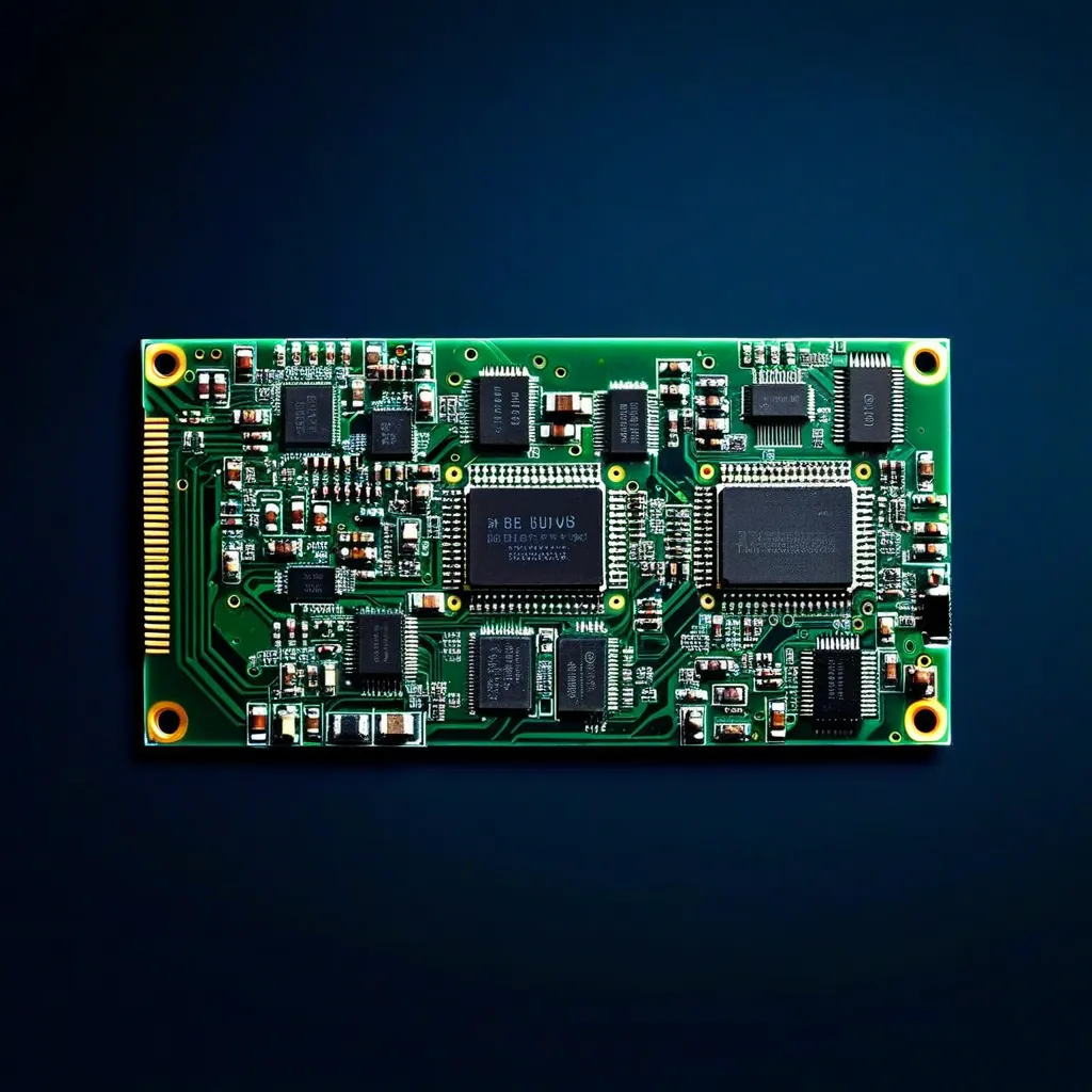
As electronic devices continue shrinking while packing more functionality, HDI PCB (High-Density Interconnect) technology has become the backbone of modern hardware design. From smartphones to medical implants, HDI boards use microvias — laser-drilled holes typically ≤150 µm in diameter — to route signals between layers in minimal space.
But not all microvias are created equal. The choice between stacked and staggered configurations has profound implications for manufacturing yield, long-term reliability, and cost. Engineers designing for automotive, aerospace, or medical applications cannot afford to overlook this decision.
This guide breaks down the trade-offs, backed by IPC standards and real manufacturing data, so you can make the right call for your next [HDI PCB stackup design]/blog/hdi-pcb-stackup-design-advanced-en/).
What Are Stacked and Staggered Microvias?
Stacked Microvias
Stacked microvias are drilled directly on top of each other across multiple sequential lamination cycles. A 3-stack configuration, for example, connects Layer 1 to Layer 4 through three aligned microvias filled with copper.
Key characteristics:
- Minimal routing footprint (one pad serves all layers)
- Requires copper-filled vias for structural support
- Enables maximum routing density
- Higher manufacturing complexity
Staggered Microvias
Staggered microvias are offset from each other on alternating layers. Each via connects only to the adjacent layer, with short traces routing to the next staggered via.
Key characteristics:
- Larger overall footprint than stacked
- Less stringent fill requirements
- Lower manufacturing risk
- Still significantly denser than through-hole vias
Reliability Comparison: What the Data Shows
Thermal Cycling Performance
The most critical reliability differentiator is behavior under thermal stress. IPC-TM-650 Method 2.6.26 (IST — Interconnect Stress Test) reveals important patterns:
Stacked microvias (3+ levels):
- Failure rates increase significantly above 2 levels of stacking
- Copper fill voids create stress concentration points
- Thermal expansion mismatch between copper fill and surrounding dielectric causes fatigue cracking
- IPC-6012 Class 3 requires voiding <25% of via depth
Staggered microvias:
- Distribute thermal stress across offset positions
- Each individual via carries less mechanical load
- Generally pass 500+ IST cycles at Class 3 requirements
- More forgiving of minor fill imperfections
IPC-2226 Guidelines
IPC-2226 (Sectional Design Standard for HDI Printed Boards) classifies microvia structures:
| Type | Configuration | Max Levels | Typical Application |
|---|---|---|---|
| I | Single level | 1 | Consumer electronics |
| II | Staggered | 2-3 | Networking, industrial |
| III | Stacked | 2-4 | Mobile, medical |
| IV | Stacked + staggered | 3-5 | Aerospace, HPC |
Manufacturing Considerations
Copper Fill Quality
The single biggest factor in stacked microvia reliability is copper fill quality. During the [electroless copper plating process]/blog/pcb-electroless-copper-plating-process-en/), achieving void-free fill in high-aspect-ratio microvias requires precise control of:
- Plating chemistry (suppressor/accelerator/leveler balance)
- Current density profiling (pulse-reverse plating preferred)
- Via geometry (depth-to-diameter ratio ≤0.75:1 ideal)
- Surface preparation (proper [plasma desmear]/blog/pcb-plasma-desmear-process-en/))
A single void in a lower-level stacked via becomes a latent defect that may not appear until thermal cycling in the field.
Process Capability by Fab Level
Not all fabricators can reliably produce stacked microvias. The capability hierarchy:
- Standard HDI fab: 1-2 level staggered, reliable
- Advanced HDI fab: 2-level stacked, 3-level staggered
- Premium HDI fab: 3+ level stacked with proven copper fill process
At AtlasPCB, we qualify stacked microvia processes through IST testing per IPC-TM-650, with documented Cpk data for copper fill thickness uniformity.
Design Guidelines: When to Use Each
Choose Stacked Microvias When:
- Routing density is paramount — BGA escape routing with ≤0.4 mm pitch
- Signal integrity matters — shorter via stubs, lower parasitic inductance
- Board real estate is extremely limited — mobile devices, wearables
- You can accept higher cost — for premium applications (medical, aerospace)
Choose Staggered Microvias When:
- Reliability margins matter more than density — automotive, industrial controls
- Cost optimization is important — staggered is 15-30% cheaper to produce
- Your fab’s capability is uncertain — staggered is more forgiving
- 4+ layer spans are needed — stacked beyond 3 levels carries significant risk
Hybrid Approach
Many successful designs combine both: stacked microvias in critical BGA fanout areas and staggered microvias elsewhere. This optimizes cost and reliability simultaneously.
Testing and Qualification
Before committing to stacked microvias in production, verify:
- Cross-section analysis — check copper fill completeness per IPC-6012
- IST testing — minimum 500 cycles for Class 3 applications
- Microsection after reflow — simulate assembly thermal profiles (3x reflow minimum)
- Coupon design — include [impedance test coupons]/blog/pcb-impedance-coupon-testing-en/) with microvia chains
For reliability-critical applications, consider [via reliability testing]/blog/pcb-via-reliability-testing-en/) programs that include accelerated life testing under combined thermal and mechanical stress.
Cost Impact Analysis
Typical cost multipliers relative to standard 2-layer PTH construction:
- 1+N+1 staggered: 1.8–2.2x
- 2+N+2 staggered: 2.5–3.0x
- 1+N+1 stacked: 2.2–2.8x
- 2+N+2 stacked: 3.5–4.5x
- 3+N+3 stacked: 5.0–7.0x
The cost premium for stacked configurations comes primarily from additional sequential lamination cycles and the more stringent copper fill requirements.
Conclusion: Making the Right Choice
The stacked vs. staggered decision ultimately comes down to three factors: required density, reliability environment, and budget. For most designs, staggered microvias offer the best balance of density improvement and manufacturing robustness. Reserve stacked configurations for applications where routing density physically cannot be achieved any other way.
If you’re designing an HDI board and need help choosing the right microvia strategy, get a quote with your design files, and our engineering team will recommend the optimal approach for your specific application.
Frequently Asked Questions
Q: Can I stack more than 3 levels of microvias?
Technically yes, but reliability drops significantly. IPC research shows failure rates increase non-linearly above 3 stacked levels. Most manufacturers recommend a maximum of 3 stacked levels for Class 3 applications.
Q: Do stacked microvias require copper-filled vias?
Yes — stacked microvias must be copper-filled (not just plated) to provide structural support for subsequent lamination and drilling. Unfilled stacked vias will collapse or deform during lamination pressure.
Q: What’s the minimum pad size for stacked microvias?
Typically 250–300 µm capture pad diameter for a 100 µm microvia drill, depending on registration tolerance. The [PCB via size selection guide]/blog/pcb-via-size-selection-guide-en/) covers detailed calculations.
Ready to start your project? Upload your Gerbers for a free engineering review, or talk to an engineer about your HDI design requirements.
Further Reading
- [PCB Via Reliability Testing: IST, Thermal Cycling, and IPC-6012 Compliance for Microvias]/blog/pcb-via-reliability-testing/)
- [PCB Rigid-Flex Bend Zone Reliability: Design Rules, Material Selection & Lifecycle Testing]/blog/pcb-rigid-flex-bend-zone-reliability/)
- [HDI PCB Design for 5G Antenna Integration: Signal Integrity Challenges in Millimeter-Wave Applications]/blog/hdi-5g-antenna-integration-pcb-design/)
- [ENEPIG vs ENIG Surface Finish: Complete Comparison for Wire Bonding, Solderability, and Long-Term Reliability]/blog/enepig-vs-enig-surface-finish-wire-bonding/)
- [HDI PCB Design Guide: Stackup Rules, Via Structures & DFM Checklist]/blog/hdi-pcb-design-guide/)
- Our Manufacturing Capabilities
About AtlasPCB — We specialize in complex PCB manufacturing for HDI, RF, and high-reliability applications. Explore our HDI PCB manufacturing capabilities . Every order includes free engineering review. Get your quote.
Reviewed by AtlasPCB Engineering Team — IPC-certified manufacturing specialists with 15+ years of production experience in HDI, RF, and high-reliability PCB fabrication. Content based on factory floor data and real customer design reviews.
- HDI PCB
- microvia reliability
- stacked via
- staggered via
- high-density interconnect
- via-in-pad