· AtlasPCB Engineering · Engineering · 13 min read
mmWave PCB Material Selection: Rogers vs Megtron vs LCP for 5G and 6G Applications
Compare Rogers 3003/4350B, Panasonic Megtron 7, and Liquid Crystal Polymer (LCP) for millimeter-wave PCB designs. Learn dissipation factor, Dk stability, moisture absorption, and cost trade-offs for 28-77 GHz 5G/6G antenna and front-end modules.

Introduction: Why Material Selection Makes or Breaks mmWave Designs
The millimeter-wave revolution is here. With 5G NR deploying at 28 GHz and 39 GHz bands worldwide, automotive radar operating at 77 GHz, and 6G research pushing toward sub-THz frequencies above 100 GHz, PCB material selection has become the single most critical design decision for RF engineers working above 24 GHz.
At these frequencies, every material property matters exponentially more. A loss tangent difference of 0.005 that’s negligible at 2.4 GHz translates to several dB of additional path loss per centimeter at 60 GHz—enough to destroy link budget margins in phased array antenna feeds or kill receiver sensitivity in radar front-ends.
This comprehensive guide compares three dominant material families for mmWave PCB applications: Rogers PTFE-based laminates, Panasonic Megtron 7 (and related hydrocarbon ceramics), and Liquid Crystal Polymer (LCP). If you’re new to RF PCB design, start with our [RF microwave PCB design fundamentals guide]/blog/rf-microwave-pcb-design/) before diving into material specifics. We’ll examine real measured performance data, manufacturing compatibility, cost structures, and practical design guidelines to help you make the right material choice for your specific mmWave application.
Understanding mmWave Loss Mechanisms
Before comparing materials, let’s understand what causes signal loss at millimeter-wave frequencies:
Dielectric Loss
Dielectric loss is the dominant loss mechanism at mmWave and is characterized by the dissipation factor (Df or tan δ). The relationship is straightforward:
α_d = 27.3 × f × √εr × tan δ / c (dB/unit length)
This means dielectric loss scales linearly with frequency. A material with Df = 0.004 at 10 GHz produces roughly 3× more loss at 30 GHz compared to the same trace length at 10 GHz. For phased array feed networks with 10+ cm of trace length, this accumulates rapidly.
Conductor Loss and Surface Roughness
At mmWave frequencies, conductor loss is amplified by skin effect and surface roughness. The skin depth at 28 GHz is only ~0.39 μm in copper, meaning current flows in an extremely thin layer. Standard electrodeposited (ED) copper with Rz roughness of 5-8 μm (standard profile) creates significant additional loss because the effective current path length increases.
For mmWave applications, you need:
- Very Low Profile (VLP) copper: Rz < 3 μm
- Hyper Very Low Profile (HVLP): Rz < 2 μm
- Rolled annealed (RA) copper: Rz < 0.5 μm (for LCP substrates)
Radiation and Mode Conversion Loss
At frequencies above 40 GHz, microstrip lines become increasingly lossy due to surface wave excitation and radiation. Substrate thickness must be carefully controlled—typically < λ/10—to prevent higher-order mode propagation. This limits practical substrate thickness to ~0.1-0.2 mm at 77 GHz.
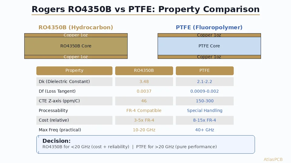
Rogers PTFE Laminates: The Gold Standard for Ultra-Low Loss
Rogers Corporation offers the most extensive portfolio of high-frequency laminates, built primarily on PTFE (polytetrafluoroethylene) and thermoset hydrocarbon chemistry.
Key Rogers Materials for mmWave
| Parameter | RO3003 | RT/duroid 5880 | RO4835 | RO4350B |
|---|---|---|---|---|
| Dk @ 10 GHz | 3.00 | 2.20 | 3.48 | 3.48 |
| Df @ 10 GHz | 0.0010 | 0.0009 | 0.0037 | 0.0037 |
| Dk @ 77 GHz | 3.02 | 2.22 | 3.54 | 3.52 |
| Moisture Absorption | 0.04% | 0.02% | 0.06% | 0.06% |
| Z-CTE (ppm/°C) | 24 | 237 | 32 | 32 |
| Processing | PTFE-specific | PTFE-specific | FR-4 compatible | FR-4 compatible |
When to Choose Rogers
Best for: Discrete RF front-end modules, phased array antenna elements, automotive radar at 77 GHz, low-volume high-performance designs, military/aerospace applications where cost is secondary to performance.
RO3003 is the workhorse for 5G antenna arrays—it offers the best balance of low loss, stable Dk, and reasonable processability among PTFE materials.
RT/duroid 5880 with its extremely low Dk of 2.20 is preferred for wide-bandwidth antenna elements where low dielectric loading enables broader impedance bandwidth.
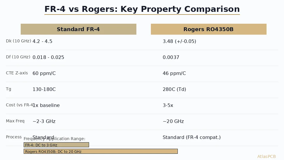
RO4350B (thermoset hydrocarbon ceramic) sacrifices some loss performance for FR-4-compatible processing, making it ideal for hybrid stackups where only select layers need high-frequency performance.
Rogers Limitations
- Cost: RO3003 is typically 15-30× more expensive than standard FR-4 per square meter
- Multilayer processing: PTFE materials require sodium etching for adhesion, special drill parameters, and fusion bonding—not all fabricators have capability
- Lead time: Specialty thicknesses often have 8-12 week material lead times
- Via reliability: High Z-CTE in some PTFE materials (RT/duroid 5880: 237 ppm/°C) creates via barrel cracking risk under thermal cycling
Panasonic Megtron 7: The Practical mmWave Choice
Megtron 7 (R-5785N) represents the latest generation of Panasonic’s low-loss laminate series, designed specifically to bridge the gap between standard FR-4 processing and high-frequency performance.
Megtron 7 Properties
- Dk: 3.37 @ 12 GHz (remarkably stable from 1-40 GHz)
- Df: 0.0015 @ 12 GHz
- Dk Stability: ±0.02 across 1-28 GHz range
- Moisture Absorption: 0.09%
- Z-CTE: 25 ppm/°C (glass transition > 230°C)
- Processing: Fully FR-4 compatible—standard drill, plating, and lamination
Why Megtron 7 Is Gaining mmWave Market Share
The key advantage of Megtron 7 is manufacturing compatibility. Any fabricator capable of processing standard multilayer FR-4 can process Megtron 7 without equipment changes. This translates to:
- Lower fabrication cost (vs Rogers PTFE): typically 3-5× FR-4 pricing vs 15-30× for Rogers
- Shorter lead times: 3-4 weeks standard, material widely stocked
- Higher layer count capability: readily available in 16-24 layer constructions
- Better via reliability: Low Z-CTE (25 ppm/°C) provides excellent PTH reliability through -55°C to +125°C cycling
For designs operating at 24-40 GHz (5G FR2 bands), Megtron 7’s Df of 0.0015 provides acceptable performance for antenna feed networks up to ~5-8 cm length. The Dk stability eliminates the need for extensive frequency-dependent impedance compensation in simulation.
Megtron 7 Limitations
- Not suitable above 50 GHz: At 60-77 GHz, the 0.0015 Df creates significant accumulated loss in longer feed networks
- Moisture sensitivity: 0.09% absorption requires conformal coating for outdoor deployments
- Glass weave effects: At mmWave, the periodic glass fiber structure creates signal skew and impedance variation (spread glass options available at premium)
Need mmWave PCB Fabrication?
AtlasPCB manufactures hybrid Rogers/Megtron stackups with HVLP copper and ±0.5 mil impedance tolerance for 5G/77GHz applications.
Get RF PCB Quote →Liquid Crystal Polymer (LCP): The Future of mmWave Substrates
LCP is emerging as arguably the ideal mmWave substrate material, particularly for antenna-in-package (AiP) and integrated module applications. Originally developed for flexible circuit applications, LCP’s unique molecular structure delivers exceptional high-frequency performance.
LCP Properties
- Dk: 2.9-3.1 @ 10-110 GHz (remarkably flat across frequency)
- Df: 0.002 @ 10 GHz, 0.003-0.004 @ 77 GHz
- Moisture Absorption: 0.02-0.04% (best-in-class)
- CTE: 17 ppm/°C in X-Y plane (matches silicon and ceramics)
- Thickness range: 25-200 μm (ideal for thin mmWave substrates)
- Processing: Requires specialized flex circuit fabrication techniques
LCP’s Killer Advantage: Moisture Stability
For outdoor 5G infrastructure and automotive radar permanently exposed to environmental cycling, LCP’s near-zero moisture absorption is transformative. While Rogers PTFE materials also have low absorption (0.02%), LCP additionally offers:
- No desorption bake required before assembly (saves process step and cost)
- Zero Dk drift between 0-95% relative humidity environments
- No popcorn effect during lead-free reflow (critical for AiP applications)
LCP for Antenna-in-Package (AiP)
The combination of thin form factor (50-100 μm per layer), low Dk, and excellent dimensional stability makes LCP the preferred substrate for mmWave AiP modules. Companies like Qualcomm (QTM545), Samsung, and MediaTek use LCP-based substrates for their 5G mmWave antenna modules integrated directly into smartphone housings.
In these applications, LCP enables:
- 4-8 layer buildup with total thickness < 0.4 mm
- Patch antenna elements with > 80% radiation efficiency at 28 GHz
- -40°C to +85°C operation without Dk calibration
- Conformal integration against device chassis without detuning
LCP Limitations
- Limited fabricator availability: Few companies worldwide can process multilayer LCP with tight registration
- Bonding challenges: Layer-to-layer bonding requires careful thermal profiling (LCP melts at 280-315°C depending on grade)
- Panel size: Typically limited to 12” × 18” panels vs 18” × 24” for standard PCB
- Cost: Comparable to Rogers PTFE for the material itself, but fabrication premiums are higher due to specialized processing
Head-to-Head Comparison: 28 GHz 5G Antenna Array
Let’s compare the three material families for a practical design: an 8×8 patch antenna array for 5G NR at 28 GHz with Butler matrix feed network.
Design Parameters
- Operating frequency: 26.5-29.5 GHz
- Array size: 8×8 = 64 elements
- Feed network length: ~12 cm (longest path from input to corner element)
- Layer count: 6 layers (2 antenna + 2 feed + ground + power)
- Production volume: 10,000 units/year
Performance Comparison
Total feed network insertion loss (12 cm path):
- Rogers RO3003: 2.1 dB
- Megtron 7: 3.8 dB
- LCP (50 μm layer): 2.9 dB
Impedance variation over -40°C to +85°C:
- Rogers RO3003: ±1.2 Ω (50 Ω nominal)
- Megtron 7: ±0.8 Ω
- LCP: ±0.6 Ω
Dk variation with humidity (30% to 90% RH):
- Rogers RO3003: < 0.01 (negligible)
- Megtron 7: 0.03-0.05
- LCP: < 0.005 (negligible)
Unit fabrication cost (6-layer, 50mm × 50mm):
- Rogers RO3003: $18-25/unit
- Megtron 7: $6-9/unit
- LCP: $15-22/unit
Verdict by Application
| Application | Recommended Material | Rationale |
|---|---|---|
| 5G base station AAS | Rogers RO3003 | Lowest loss for long feed networks; cost acceptable at infrastructure pricing |
| 5G smartphone AiP | LCP | Thin profile, humidity stability, AiP integration |
| 77 GHz auto radar | Rogers RO3003/RT5880 | Ultra-low loss critical for FMCW range resolution |
| 5G CPE/FWA | Megtron 7 | Cost-performance balance for consumer equipment |
| Satellite com (LEO) | Rogers + LCP hybrid | Space-grade reliability with minimum mass |
| Drone radar | Megtron 7 hybrid | Weight-sensitive, moderate performance adequate |
Hybrid Stackup Design: Best of All Worlds
In practice, most production mmWave designs use hybrid stackups combining multiple materials. This approach optimizes cost while maintaining performance where it matters.
Example: 10-Layer Hybrid for 28 GHz Phased Array
Layer 1:  Antenna patches     → RO3003 (0.127 mm)
          Prepreg bond        → Rogers 2929 bondply
Layer 2:  Antenna ground      → RO3003 (0.127 mm)
          Prepreg             → Megtron 7 prepreg
Layer 3:  RF feed network     → Megtron 7 core (0.1 mm)
Layer 4:  RF ground           → Megtron 7 core
Layer 5:  Digital/control     → Standard FR-4
Layer 6:  Power plane         → Standard FR-4
Layer 7:  Digital signals     → Standard FR-4
Layer 8:  Ground              → Megtron 7 core (0.1 mm)
Layer 9:  RF distribution     → Megtron 7 core
Layer 10: Connector interface → RO4350B (0.254 mm)
Hybrid Stackup Design Rules
- CTE matching: Keep Z-CTE mismatch between adjacent materials < 15 ppm/°C to prevent delamination
- Drill aspect ratio: Limit to 8:1 for through-holes spanning hybrid materials; use sequential lamination for higher aspect ratios
- Registration: Expect ±50 μm layer-to-layer registration through dissimilar materials (vs ±25 μm in homogeneous stackups)
- Bonding: Use compatible prepreg systems—Rogers 2929 for PTFE-to-PTFE, Megtron 7 prepreg for hydrocarbon interfaces
- Thermal relief: Add thermal relief pads at material boundaries to reduce thermo-mechanical stress on vias
Manufacturing Considerations
Fabricator Capability Requirements
When selecting a fabricator for mmWave PCBs, verify these capabilities:
For Rogers PTFE:
- Sodium naphthalenide or plasma surface treatment capability
- Controlled-depth drilling (for blind vias in multilayer PTFE)
- Fusion bonding temperature control (±2°C across panel)
- PTFE-compatible drill parameters (slower feed, sharper bits)
For Megtron 7:
- Standard multilayer capability (most advanced shops qualify)
- Spread glass prepreg availability (for skew-sensitive designs)
- HVLP copper foil lamination experience
- Sequential lamination if layer count > 12
For LCP:
- Specialized flex/rigid-flex fabrication line
- Laser drilling capability (UV laser preferred for LCP)
- Thermocompression bonding with precise temperature profiling
- Clean room processing (LCP is particle-sensitive)
For a deeper dive into impedance design, see our guide on [controlled impedance PCB stackup calculations]/blog/controlled-impedance-pcb-design-stackup-calculations/).
Impedance Control at mmWave
Achieving ±5% impedance tolerance at mmWave requires tighter process controls than standard PCB fabrication:
- Etch factor control: ±5 μm trace width tolerance (vs ±15 μm standard)
- Dielectric thickness: ±5% or ±0.005 mm (vs ±10% standard)
- Copper thickness: ±2 μm after plating
- Surface roughness specification: Must specify Rz and Ra for each copper layer
At AtlasPCB, our RF PCB manufacturing process includes TDR verification of impedance on every panel, with test coupons designed to match your specific stackup and geometry.
Design Guidelines for mmWave PCB Layout
Transmission Line Selection
Microstrip (signal on top, ground below):
- Simple, single-sided etching
- Accessible for component mounting
- Higher radiation loss above 40 GHz
- Substrate thickness < λ/10 required
Grounded Coplanar Waveguide (GCPW):
- Better field confinement than microstrip
- Lower radiation loss at 60-77 GHz
- Ground coplanar gaps provide additional Dk insensitivity
- Preferred for most mmWave designs above 40 GHz
Substrate Integrated Waveguide (SIW):
- Lowest loss for long interconnects at 60+ GHz
- Via fence creates waveguide boundaries
- Large footprint but excellent isolation
- Ideal for antenna feed networks above 50 GHz
Via Transitions
Via transitions between layers add 0.1-0.5 dB per transition at mmWave frequencies if not properly designed. Key rules:
- Anti-pad clearance: Minimize to reduce parasitic capacitance (0.1 mm typical)
- Back-drill stubs: Remove unused via stubs—even 0.2 mm stubs create significant resonances at 28 GHz
- Ground via fencing: Place ground vias within λ/4 of signal vias for mode suppression
- Pad-less vias: Use where possible to minimize discontinuity capacitance
Antenna Element Integration
For patch antennas integrated on the PCB:
- Patch dimensions scale as λ/2 in the dielectric (e.g., ~2.9 mm at 28 GHz on Dk=3.0 material)
- Minimum patch-to-patch spacing: λ₀/2 for grating lobe suppression (~5.4 mm at 28 GHz)
- Probe feed via position determines input impedance (typically 1/3 from edge for 50 Ω)
- Consider aperture-coupled feeding for wider bandwidth (>15%)
Cost Optimization Strategies
Panel Utilization
mmWave modules are typically small (20-60 mm per side). Maximize panel utilization by:
- Designing to standard panel sizes (18” × 24” for FR-4/Megtron, 12” × 18” for Rogers)
- Including test coupons within the array border
- Allowing 5 mm minimum spacing between units for routing and breakaway
Volume Pricing Breakpoints
Material costs drop significantly at volume. Typical pricing curves:
- Rogers RO3003 (0.127 mm): $1,200/m² at prototype → $600/m² at 100+ panels
- Megtron 7 (0.1 mm): $180/m² at prototype → $90/m² at 100+ panels
- LCP (50 μm): $800/m² at prototype → $450/m² at 100+ panels
When to Use Each Approach
- < 100 units: Use Rogers—performance matters more than cost at prototype stage
- 100-10,000 units: Evaluate Megtron 7 hybrid—significant cost savings if performance meets spec
- > 10,000 units: LCP or custom Megtron 7 stackup optimized for your specific design
- > 100,000 units: Consider custom laminate development with material suppliers
Future Trends: Materials for 6G and Beyond
As research pushes toward 6G frequencies (100-300 GHz, sub-THz), new materials are emerging:
Glass Substrates
Corning and AGC are developing ultra-thin glass (50-100 μm) with Dk ~5.5 and Df < 0.003 at 100+ GHz. Glass offers:
- Perfect surface smoothness (no copper roughness contribution)
- Excellent dimensional stability
- Through-glass vias (TGV) for 3D integration
- Compatible with semiconductor-style wafer processing
Additive Manufactured Dielectrics
3D-printed dielectric structures enable complex waveguide geometries impossible with laminate PCB:
- Photopolymer resins with Dk < 3.0 and Df < 0.005 up to 300 GHz
- Gradient dielectric structures for lens antennas
- Integrated air cavities for SIW performance in compact form factors
Organic Interposers
Bridge technologies between PCB and semiconductor substrates:
- 5-10 μm line/space capability on organic substrate
- Direct die attach without wire bonds or flip-chip bumps
- Compatible with existing OSAT packaging flows
- Dk targeting 3.0-3.3 with Df < 0.003 at 77 GHz
Conclusion: Making the Right Material Choice
There is no single “best” material for mmWave PCBs. The optimal choice depends on your specific constraints:
Choose Rogers PTFE when loss budget is critical, you’re working above 50 GHz, volume is low-to-moderate, and your fabricator has PTFE processing capability.
Choose Megtron 7 when cost-performance balance matters, you need high layer counts, your design operates at 24-40 GHz, and standard FR-4 processing compatibility is required.
Choose LCP when moisture resistance is essential, you need thin/flexible form factors, the application is AiP or module integration, and you have access to specialized flex fabricators.
Choose hybrid when different sections of your design have different requirements—which is almost always the case in real-world systems.
Whatever material you select, ensure your fabricator has documented experience with that specific material at your target frequency. Request test data on actual production panels, not just datasheet values—real-world performance varies significantly with processing conditions.
Need help selecting materials for your mmWave PCB project? Our RF engineering team has fabricated 5G antenna arrays for major telecom OEMs and can recommend the optimal stackup for your frequency band and performance requirements. Contact our RF team for a design review.
Further Reading
- [Rogers PCB Fabrication: Material Sourcing, Lead Times & Quality Control]/blog/rogers-pcb-fabrication/)
- [RF PCB Material Selection for Automotive Radar: Rogers vs PTFE Performance Analysis at 77-81 GHz]/blog/automotive-radar-pcb-materials-rogers-ptfe-analysis/)
- [PCB Design for GaN and SiC Power Devices: Thermal Management, Layout Rules, and Material Selection]/blog/pcb-design-gan-sic-power-devices-thermal-layout/)
- [PCB Panelization and Array Design: V-Score vs Tab Routing, DFM Rules, and Cost Optimization]/blog/pcb-panelization-v-score-tab-routing-dfm-cost-optimization/)
- [PCB Rigid-Flex Bend Zone Reliability: Design Rules, Material Selection & Lifecycle Testing]/blog/pcb-rigid-flex-bend-zone-reliability/)
- Material Options & Capabilities
About AtlasPCB — We specialize in complex PCB manufacturing for HDI, RF, and high-reliability applications. Explore our RF and high-frequency PCB services . Every order includes free engineering review. Get your quote.
Reviewed by AtlasPCB Engineering Team — IPC-certified manufacturing specialists with 15+ years of production experience in HDI, RF, and high-reliability PCB fabrication. Content based on factory floor data and real customer design reviews.
- mmWave
- 5G PCB
- 6G
- Rogers
- Megtron 7
- LCP
- RF materials
- high-frequency PCB
- antenna array
- low-loss laminate