· AtlasPCB Engineering · Engineering · 9 min read
High-Frequency PCB Design Best Practices: RF/Microwave Layout, Ground Planes, Via Fencing, and Transition Design
Master RF and microwave PCB layout techniques including ground plane management, via fencing for isolation, coplanar waveguide transitions, and connector launch design. Covers frequencies from 1 GHz to 77 GHz.

Radio frequency (RF) and microwave PCB design operates under stricter rules than digital layout. At high frequencies, every trace is a transmission line, every via is a discontinuity, and every ground plane gap creates radiation. This guide covers the essential best practices for designing PCBs that operate reliably from 1 GHz through millimeter-wave (mmWave) frequencies.
Understanding RF Transmission Lines on PCB
At RF frequencies, signal behavior is governed by electromagnetic wave propagation, not lumped-circuit models. The three primary transmission line structures on PCB are:
Microstrip
A trace on the outer layer with a ground plane on the adjacent layer. This is the most common RF transmission line.
- Impedance range: 25–120 Ω (practical)
- Effective Dk: Lower than substrate Dk due to partial air dielectric
- Radiation: Higher than stripline; increases with frequency
- Dispersion: Moderate; effective Dk varies with frequency
Stripline
A trace embedded between two ground planes. Offers better shielding and lower radiation.
- Impedance range: 30–120 Ω
- Effective Dk: Equal to substrate Dk (fully enclosed in dielectric)
- Radiation: Very low (shielded)
- Dispersion: Lower than microstrip
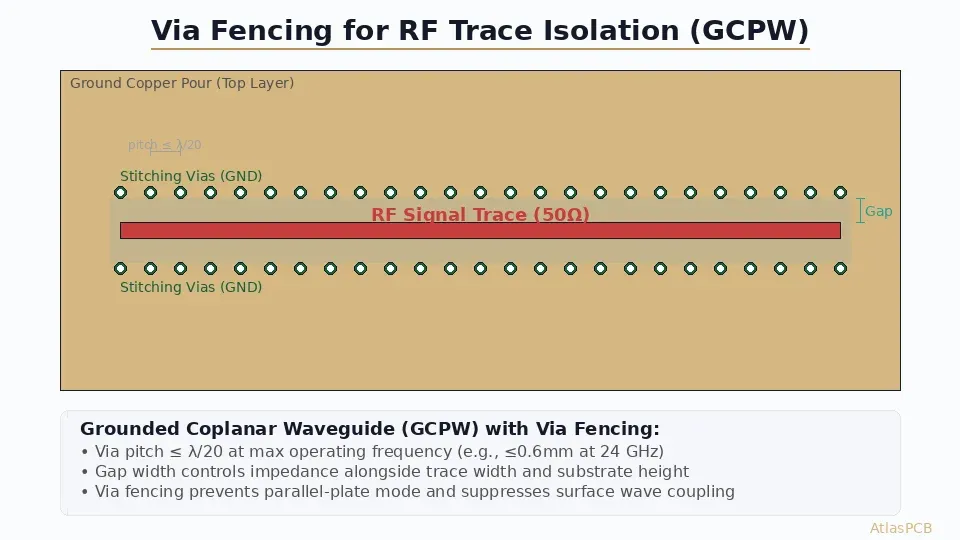
Coplanar Waveguide (CPW/GCPW)
A trace on the outer layer flanked by ground copper on the same layer, typically with a ground plane below (grounded CPW or GCPW).
- Impedance range: 30–100 Ω
- Effective Dk: Between microstrip and stripline
- Radiation: Low (ground coplanar copper provides shielding)
- Dispersion: Moderate
- Advantage: Easier component mounting, good for mmWave
For a detailed comparison, see our [microstrip vs. stripline guide]/blog/microstrip-vs-stripline/).
| Parameter | Microstrip | Stripline | GCPW |
|---|---|---|---|
| Shielding | Low | High | Medium-High |
| Insertion loss | Medium | Low-Medium | Medium |
| Radiation | High at >10 GHz | Very low | Low |
| Manufacturing ease | Easy | Medium | Medium |
| Component access | Direct | Requires via transition | Direct |
| mmWave suitability | Fair | Good | Excellent |
Ground Plane Management
The ground plane is arguably the most important element in RF PCB design. It serves as the current return path, electromagnetic shield, and impedance reference.
Rule 1: Continuous Ground Under RF Traces
Never route signals or power traces on the ground reference layer directly beneath an RF trace. Any gap, slot, or discontinuity in the ground plane forces return current to detour, creating inductance and radiation.
Quantifying the impact: A 1 mm slot in the ground plane beneath a 50 Ω microstrip at 5 GHz can cause:
- 2–5 dB additional insertion loss at the slot
- 10–15 dB degradation in return loss
- Significant EMI radiation at the slot edges
Rule 2: Ground Plane Stitching Vias
Connect all ground planes together with stitching vias throughout the board. Recommended stitching via spacing:
| Frequency Range | Max Via Spacing | Via Diameter |
|---|---|---|
| < 3 GHz | 3.0 mm | 0.3 mm |
| 3–10 GHz | 1.5 mm | 0.25 mm |
| 10–30 GHz | 0.8 mm | 0.2 mm |
| 30–77 GHz | 0.4 mm | 0.15 mm |
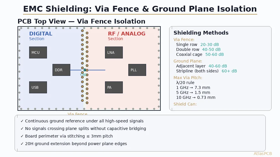
Rule 3: Split Ground Planes — Avoid or Manage Carefully
In mixed-signal designs, the traditional advice is to split analog and digital ground planes. In RF designs, this is often counterproductive. A split creates a slot antenna at the split boundary.
Better approach: Use a unified ground plane with careful component placement. Separate RF, digital, and power sections by physical location, not by ground plane splits. If a split is absolutely necessary, bridge it with multiple capacitors (100 pF–10 nF) at close spacing.
Rule 4: Ground Copper Pour on Signal Layers
Fill unused areas on signal layers with ground copper, stitched to the ground plane with vias at ≤λ/20 spacing. This reduces coupling between traces and provides additional shielding.
Caution: Ensure ground copper pour does not create narrow channels or peninsulas near RF traces, which can act as resonant structures. Maintain at least 3× trace width clearance between RF traces and unrelated copper pour.
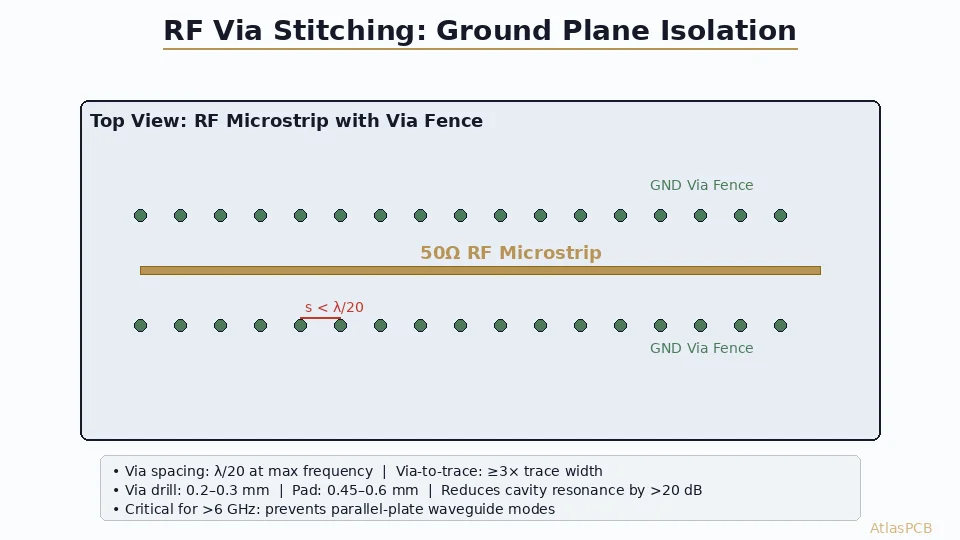
Via Fencing for RF Isolation
Via fencing (also called via shielding or via walls) creates a Faraday cage around RF traces using rows of ground vias. This is essential for:
- Isolating RF channels to prevent crosstalk
- Preventing surface wave propagation between circuits
- Containing electromagnetic fields in stripline structures
Via Fence Design Rules
- Via spacing: ≤λ/20 at the highest frequency of concern (including harmonics)
- Via diameter: Standard 0.2–0.3 mm; smaller vias for higher frequencies
- Via-to-trace spacing: ≥3× dielectric thickness from the RF trace edge to the nearest via fence via
- Via rows: Single row provides ~20 dB isolation; double row provides ~40 dB
- Via connection: Every fence via must connect to ground planes on both sides of the signal layer
Practical Example: 28 GHz 5G Front-End
For a 28 GHz 5G module on Rogers RO4350B (Dk = 3.48):
- Wavelength in dielectric: λ = c / (f × √Dk) = 300 / (28 × √3.48) ≈ 5.74 mm
- Via spacing: λ/20 = 0.29 mm → use 0.25 mm spacing
- Via diameter: 0.15 mm (laser drilled)
- Double fence rows on each side of GCPW traces
- Fence connects Layer 1 ground coplanar to Layer 2 ground plane
This configuration provides >40 dB isolation between adjacent RF channels at 28 GHz.
Transition Design
RF signals often need to transition between different transmission line types—microstrip to stripline, PCB trace to connector, or PCB to component pad. Each transition is a potential source of reflection and loss.
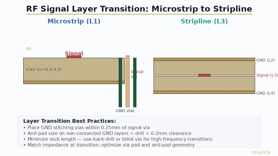
Microstrip-to-Stripline Transition
This transition occurs when an RF signal moves from an outer layer to an inner layer via a via.
Best practices:
- Via optimization: Use a via diameter no larger than necessary. For frequencies >10 GHz, use microvias or HDI blind vias.
- Back-drilling: For through-hole vias, back-drill the unused stub portion. A 1 mm via stub creates a quarter-wave resonance at ~37 GHz (in FR-4), causing a catastrophic null in the S21 response. Learn more about this in our [back-drill guide]/blog/pcb-back-drill/).
- Anti-pad sizing: The via anti-pad on non-reference ground layers should be as small as possible (typically pad diameter + 0.2 mm).
- Ground vias: Place 3–4 ground return vias within 0.5 mm of the signal via, connecting the microstrip ground layer to the stripline ground layers.
- Impedance matching: Adjust trace width on both sides of the transition to maintain 50 Ω (or target impedance) through the via region.
Connector Launch Design
The PCB-to-connector interface is often the dominant source of return loss in an RF system. Key design considerations:
SMA/SMP connectors (DC–18 GHz):
- Pad dimensions per connector manufacturer datasheet
- Ground vias in a semicircle around the signal pad, spaced ≤1.0 mm
- Controlled impedance taper from connector pad to trace
- Anti-pad on inner ground layers sized for 50 Ω
2.92 mm / 2.4 mm / 1.85 mm connectors (DC–40/50/67 GHz):
- Tighter via fence around launch (0.3–0.5 mm spacing)
- Thinner substrates (4–8 mil) for better impedance control
- GCPW launch preferred over pure microstrip
- Via-less transition where possible (edge-launch connectors)
Component Pad Transitions
RF components (amplifiers, filters, mixers) have specific pad geometries that may not match your transmission line width. Design a gradual taper:
- Taper length: ≥λ/10 for return loss <20 dB
- Taper shape: Linear or Klopfenstein (optimized) taper
- Ground continuity: Maintain ground pad connections immediately adjacent to signal pads
Substrate Material Selection
Material choice is critical at high frequencies. The two key parameters are:
- Dk (Dielectric Constant): Determines impedance and wavelength. Lower Dk → wider traces for given impedance → easier manufacturing.
- Df (Dissipation Factor / Loss Tangent): Determines dielectric loss. Lower Df → lower insertion loss.
Material Comparison for RF Applications
| Material | Dk @ 10 GHz | Df @ 10 GHz | Max Freq | Cost |
|---|---|---|---|---|
| Standard FR-4 | 4.2–4.5 | 0.020–0.025 | ~5 GHz | 1× |
| Low-loss FR-4 (Megtron 6) | 3.6 | 0.004 | ~15 GHz | 2× |
| Rogers RO4350B | 3.48 | 0.0037 | ~30 GHz | 3–4× |
| Rogers RO4003C | 3.38 | 0.0027 | ~40 GHz | 3–4× |
| Rogers RT/duroid 5880 | 2.20 | 0.0009 | 77 GHz+ | 5–8× |
| Rogers RO3003 | 3.00 | 0.0013 | 77 GHz+ | 5–7× |
For more on substrate selection, see our comprehensive [Dk/Df substrate guide]/blog/high-frequency-pcb-substrate-selection-dk-df/).
Hybrid Stackups
For cost optimization, use RF-grade materials only where needed:
- RF layers: Rogers or PTFE-based laminate for signal and adjacent ground layers
- Digital/power layers: Standard FR-4 for non-RF routing and power distribution
- Bonding: Use compatible prepreg (e.g., Rogers 4450F) to bond dissimilar materials
Example 6-layer hybrid stackup:
L1 (RF signal)      — RO4350B, 8 mil
L2 (Ground)         —
L3 (Digital signal)  — FR-4, 8 mil
L4 (Power)          —
L5 (Ground)         —
L6 (RF signal)      — RO4350B, 8 mil
Layout Best Practices Summary
Trace Routing
- Minimize trace length: Every millimeter adds insertion loss. At 28 GHz on RO4350B, loss is approximately 0.15 dB/mm for a 50 Ω microstrip.
- Avoid bends: If bends are necessary, use curved (arc) bends or chamfered 45° corners. Right-angle bends create impedance discontinuities.
- Consistent trace width: Maintain calculated trace width throughout the RF path. Even a 10% width variation causes measurable return loss above 10 GHz.
- Trace separation: Maintain ≥3× dielectric thickness between parallel RF traces (≥5× for >20 dB isolation).
- Avoid crossing RF traces: On different layers, RF traces should cross at 90° with ground plane separation, or not at all.
Component Placement
- Partition the board: Group RF, digital, and power sections physically. RF section should be closest to connectors/antennas.
- Short RF paths: Place RF components to minimize trace lengths in the signal chain.
- Decoupling: Place decoupling capacitors as close as possible to RF IC power pins, on the same layer if possible.
- Thermal management: RF power amplifiers generate significant heat. Provide thermal vias to internal ground/power planes and ensure adequate copper area for heat spreading.
Manufacturing Considerations
- Specify Dk tolerance: For impedance-sensitive designs, specify Dk tolerance to ±2% or tighter.
- Copper roughness: At mmWave frequencies, copper surface roughness significantly increases conductor loss. Specify low-profile (LP) or very-low-profile (VLP) copper foil for traces above 20 GHz.
- Etch compensation: Fine RF traces (≤4 mil) require etch compensation. Work with your fabricator to ensure final trace width matches the design.
- Test coupons: Include impedance test coupons, insertion loss test coupons, and TDR coupon structures on the panel.
Simulation and Verification
Pre-Layout Simulation
Before routing, simulate critical parameters:
- Stackup analysis: Use 2D field solvers (e.g., Polar Si9000) to determine trace dimensions for target impedance
- Transmission line loss: Calculate expected insertion loss per unit length for the chosen material and geometry
- Via model: Simulate via transitions using 3D EM tools (HFSS, CST) for frequencies >10 GHz
Post-Layout Verification
After routing, verify:
- S-parameter extraction: Simulate complete RF paths including vias, transitions, and connector launches
- Coupling analysis: Verify isolation between adjacent RF channels meets spec
- Resonance check: Look for unintended resonances from via stubs, ground plane gaps, or parasitic cavities
Conclusion
High-frequency PCB design demands attention to electromagnetic fundamentals at every step—from stackup definition and material selection through trace routing and via placement. The practices outlined here—continuous ground planes, proper via fencing, clean transitions, and appropriate substrate materials—form the foundation for RF PCBs that meet their performance targets.
At Atlas PCB, we manufacture RF and microwave PCBs up to 77 GHz on Rogers, Taconic, and other specialty substrates. Our engineering team provides DFM feedback specific to your frequency range and design complexity. Request a quote to discuss your high-frequency PCB project.
For further reading, explore our guides on [RF PCB design guidelines]/blog/rf-pcb-design-guidelines/), [signal integrity]/blog/signal-integrity-pcb-design-guide/), and [impedance matching for differential pairs]/blog/pcb-impedance-matching-differential-pairs/).
Further Reading
- [HDI PCB Design Guide: Stackup Rules, Via Structures & DFM Checklist]/blog/hdi-pcb-design-guide/)
- [HDI PCB Technology: Microvias, Laser Drilling, and High-Density Design]/blog/hdi-pcb-technology/)
- [Blind Via vs Buried Via: Design Rules, Cost Impact & When to Use Each]/blog/blind-via-vs-buried-via/)
- [Controlled Impedance PCB: Design, Stackup & Testing Explained]/blog/controlled-impedance-pcb/)
- [High-Speed PCB Design: Signal Integrity Essentials for Modern Electronics]/blog/high-speed-pcb-design/)
About AtlasPCB — We specialize in complex PCB manufacturing for HDI, RF, and high-reliability applications. Explore our RF and high-frequency PCB services, or get an impedance-controlled PCB manufacturing . Every order includes free engineering review. Get your quote.
Reviewed by AtlasPCB Engineering Team — IPC-certified manufacturing specialists with 15+ years of production experience in HDI, RF, and high-reliability PCB fabrication. Content based on factory floor data and real customer design reviews.
- RF PCB
- high frequency
- microwave
- via fencing
- ground plane
- impedance