· AtlasPCB Engineering · Engineering · 10 min read
PCB Impedance Matching and Differential Pair Design: Spacing, Length Matching, and Layout
A comprehensive guide to differential pair PCB design covering impedance matching techniques, pair spacing optimization, length matching strategies, routing topologies, and practical design rules for high-speed serial interfaces including PCIe, USB4, and Ethernet.
Differential signaling is the foundation of modern high-speed digital communication. PCIe, USB4, Thunderbolt, HDMI, Ethernet, and LVDS all use differential pairs to achieve high data rates with excellent noise immunity. Designing differential pairs that meet impedance, skew, and loss specifications requires understanding the physics of coupled transmission lines and translating that understanding into practical layout rules.
Differential Pair Fundamentals
Why Differential Signaling?
In differential signaling, information is encoded as the voltage difference between two complementary signals (P and N, or + and −). Key advantages:
- Common-mode noise rejection: External noise couples equally to both traces and is rejected by the differential receiver
- Lower EMI radiation: The opposing currents in P and N traces create opposing electromagnetic fields that partially cancel
- Reduced return current dependency: Differential pairs are less sensitive to ground plane discontinuities than single-ended signals (though good ground practice is still important)
- Doubled voltage swing: Effective signal swing is 2× the single-ended amplitude, improving SNR
Coupled vs. Uncoupled Trace Behavior
When two traces run in parallel proximity, their electromagnetic fields interact (couple). This coupling changes the effective impedance:
- Even mode: Both traces driven with the same signal (common mode). Fields reinforce. Impedance increases: Z_even > Z_0.
- Odd mode: Traces driven with opposite signals (differential mode). Fields partially cancel between the traces. Impedance decreases: Z_odd < Z_0.
Key relationships:
- Z_diff = 2 × Z_odd (differential impedance)
- Z_common = Z_even / 2 (common-mode impedance)
- For uncoupled traces: Z_odd ≈ Z_even ≈ Z_0, so Z_diff ≈ 2 × Z_0
- For tightly coupled traces: Z_odd < Z_0, so Z_diff < 2 × Z_0
Impedance Targets by Interface
| Interface | Z_diff Target (Ω) | Tolerance | Data Rate |
|---|---|---|---|
| PCIe Gen 4 | 85 | ±15% | 16 GT/s NRZ |
| PCIe Gen 5 | 85 | ±10% | 32 GT/s NRZ |
| PCIe Gen 6 | 85 | ±10% | 64 GT/s PAM4 |
| USB 3.2 | 90 | ±10% | 10 Gbps |
| USB4 / Thunderbolt 4 | 85–90 | ±10% | 40 Gbps |
| HDMI 2.1 | 100 | ±10% | 48 Gbps |
| 10G/25G Ethernet | 100 | ±10% | 10/25 Gbps NRZ |
| 100G Ethernet (4×25G) | 100 | ±10% | 25 Gbps NRZ |
| 400G Ethernet (4×100G) | 92–100 | ±10% | 53.125 Gbps PAM4 |
| DDR5 (DQ) | 40–50 SE | ±10% | 4.8–8.4 GT/s |
| LVDS | 100 | ±10% | 0.655 Gbps |
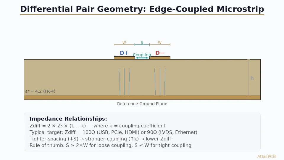
Impedance Calculation
Differential impedance is calculated using 2D field solvers that account for the complete cross-sectional geometry:
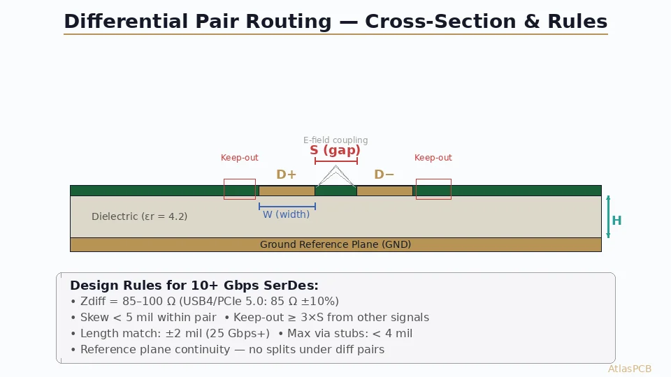
Key Variables
- Trace width (w): Primary impedance control parameter
- Trace spacing (s): Gap between P and N traces (edge-to-edge)
- Dielectric height (h): Distance to reference plane(s)
- Dielectric constant (Dk): Material property
- Copper thickness (t): Finished copper thickness
- Etch factor: Trapezoidal trace cross-section from subtractive etching
Edge-Coupled Stripline (Most Common for Differential Pairs)
For edge-coupled stripline between two ground planes:
Approximate formula (for quick estimation only):
Z_diff ≈ 2 × Z_0 × (1 - 0.48 × e^(-0.96 × s/h))
Where Z_0 is the uncoupled single-ended stripline impedance.
Example: Z_0 = 55Ω, s/h = 1.0: Z_diff ≈ 2 × 55 × (1 - 0.48 × e^(-0.96)) = 110 × (1 - 0.48 × 0.383) = 110 × 0.816 = 89.8Ω
For production designs, always use a 2D field solver (Polar Si9000, Cadence Sigrity, Ansys Q2D). Approximate formulas do not account for etch factor, soldermask, or asymmetric dielectrics.
Coupling Factor (kc)
The coupling factor quantifies how tightly coupled the pair is:
kc = (Z_even - Z_odd) / (Z_even + Z_odd)
| kc Range | Coupling Level | Typical s/h Ratio |
|---|---|---|
| 0.00–0.05 | Loosely coupled | s/h > 3.0 |
| 0.05–0.15 | Moderately coupled | s/h = 1.0–3.0 |
| 0.15–0.30 | Tightly coupled | s/h = 0.5–1.0 |
| 0.30+ | Very tightly coupled | s/h < 0.5 |
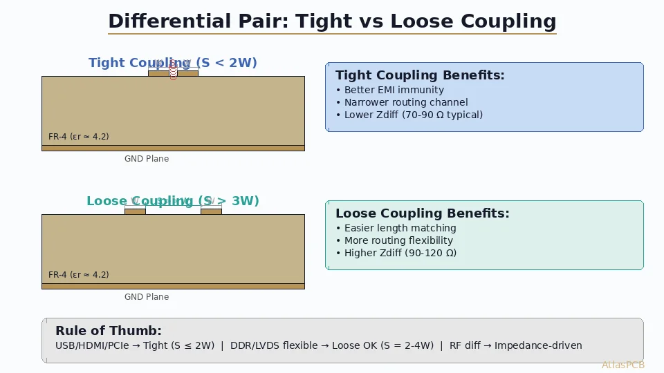
Trade-offs:
- Tight coupling (small s/h): Better common-mode rejection, lower EMI, but traces are closer together—harder to route and more sensitive to manufacturing variation
- Loose coupling (large s/h): Easier routing, more tolerant of manufacturing variation, but less common-mode rejection and wider channel footprint
For our detailed guide on impedance control, see [controlled impedance PCB]/blog/controlled-impedance-pcb/).
Pair Spacing Design
Intra-Pair Spacing (Gap Between P and N)
The gap between P and N traces must be consistent throughout the route to maintain consistent differential impedance.
Design rules:
- Hold spacing constant: Maintain the designed gap (typically 1–2× trace width) within ±10%
- Minimum spacing: Per fabrication capability (usually ≥75 µm / 3 mil)
- At pads and vias: Spacing changes are unavoidable at component pads and via transitions. Keep the non-standard-spacing length as short as possible.
Inter-Pair Spacing (Between Adjacent Pairs)
The distance between two different differential pairs determines crosstalk between them.
| Spacing (× dielectric height H) | Pair-to-Pair Crosstalk |
|---|---|
| 3H | ~2–5% NEXT |
| 4H | ~1–2% NEXT |
| 5H | <1% NEXT |
Practical recommendation: Maintain ≥4× dielectric height between adjacent differential pairs for most high-speed interfaces. For very sensitive links (56G PAM4), use ≥5H.
Length Matching
Intra-Pair Length Matching (P vs. N Skew)
The P and N traces of a differential pair must be matched in length to minimize timing skew between them. Skew converts to common-mode noise at the receiver, degrading signal quality.
Skew budget by data rate:
| Data Rate | Max Intra-Pair Skew (time) | Max Skew (length in FR-4) |
|---|---|---|
| 5 Gbps NRZ | 10 ps | 1.5 mm |
| 10 Gbps NRZ | 5 ps | 0.75 mm |
| 25 Gbps NRZ | 3 ps | 0.45 mm |
| 56 Gbps PAM4 | 1.5 ps | 0.23 mm |
| 112 Gbps PAM4 | 1.0 ps | 0.15 mm |
Sources of skew:
- Bends: When a pair turns a corner, the outer trace is longer than the inner trace. A 90° turn with 6 mil gap creates approximately 9.4 mil (0.24 mm) skew per turn.
- Via transitions: Different via pad locations for P and N can introduce skew.
- Component pin assignment: Non-symmetric pin positions create inherent skew that must be compensated.
Intra-Pair Length Matching Techniques
Serpentine (meander) compensation:
After each bend or skew-inducing feature, add a small serpentine on the shorter trace to equalize length.
Serpentine design rules:
- Amplitude (height): ≥2× trace width to avoid self-coupling
- Gap between serpentine segments: ≥4× trace width (to prevent self-crosstalk within the serpentine)
- Placement: Immediately after the skew source, not accumulated at the end
- Style: Use smooth curves (arc bends), not sharp corners
Inter-Pair Length Matching (Lane-to-Lane)
For parallel bus interfaces (PCIe x16, multi-lane Ethernet), each differential pair lane must also be matched to other lanes to within a specified tolerance:
| Interface | Inter-Pair Match |
|---|---|
| PCIe Gen 4/5 | ±12.7 mm (500 mils) |
| USB 3.2 TX to RX | ±2.0 mm |
| DDR5 (byte lane) | ±1.0 mm |
| LVDS (parallel) | ±2.5 mm |
Inter-pair matching is typically much looser than intra-pair matching because the interface protocol handles lane-to-lane skew through de-skew buffers or training sequences.
Routing Topology and Best Practices
Breakout from IC/BGA
The most challenging routing region is the BGA escape area under fine-pitch components:
- Pin assignment optimization: Work with the silicon vendor’s reference design to optimize P/N pin swaps. Many interfaces allow polarity inversion, which lets you avoid crossing pairs.
- Dog-bone vs. via-in-pad: Via-in-pad with copper fill eliminates the dog-bone fanout, saving space and reducing skew. See our [via-in-pad guide]/blog/via-in-pad-design/).
- Layer transition: Transition both P and N traces through the same via structure simultaneously. Place ground return vias between and on both sides of the signal via pair.
Pair Routing Between Components
- Maintain consistent spacing: Use your EDA tool’s differential pair router to maintain the target gap automatically.
- Minimize layer transitions: Each via transition is an impedance discontinuity and adds insertion loss (0.3–1.0 dB per via pair at 10+ GHz).
- Avoid routing between the P and N traces: Never route an unrelated signal or power trace between the two traces of a differential pair. This disrupts coupling and degrades common-mode rejection.
- Guard spacing: Do not place other signals closer than 4H to either edge of the differential pair.
Bends and Corners
- Use 45° corners or arc bends for the pair. The pair should turn as a unit, maintaining constant spacing through the bend.
- Compensate length at every bend: Don’t accumulate compensation to the end of the route—correct immediately.
- Avoid routing pairs through dense via fields where the ground plane is compromised.
AC Coupling Capacitors
Many high-speed serial links require AC coupling capacitors (typically 100 nF or 10 nF, 0201 or 0402 package) in series with each lane:
- Place symmetrically: Capacitors for P and N should be placed at the same location along the route, with identical trace lengths to and from the capacitors.
- Orientation: Orient the capacitor pads along the direction of signal flow to minimize discontinuity.
- Pad geometry: Use the smallest package possible (0201 for 25+ Gbps) to minimize the stub effect of the pad structure.
- Return path: Provide ground vias near the capacitor pads.
Common Mode Management
Why Common Mode Matters
Even in a perfect differential system, some energy exists as common mode (both traces at the same voltage relative to ground). Sources include:
- Intra-pair skew: Converts differential signal to common mode
- Asymmetric coupling: Unequal distance to ground plane (trace near board edge) converts modes
- Reference plane discontinuities: Ground plane gaps convert differential to common mode
- Connector transitions: Connector pin geometry may have different impedance for differential and common modes
Common Mode Rejection Techniques
- Maintain pair symmetry: Equal trace width, equal distance to ground plane, equal pad sizes
- Common-mode choke: For off-board interfaces (USB, HDMI), a common-mode choke attenuates common-mode noise while passing differential signals
- Ground plane continuity: Continuous ground plane under the entire pair route
- Symmetrical via structures: Both P and N vias should have identical anti-pads, barrel lengths, and surrounding ground via placement
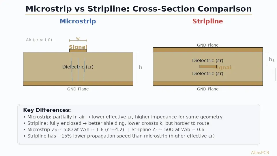
Stackup Optimization for Differential Pairs
Preferred Routing Layers
Stripline (inner layers) is strongly preferred for differential pairs because:
- Two reference planes provide better shielding
- Zero far-end crosstalk in homogeneous dielectric
- Better impedance control due to enclosed geometry
- Lower EMI radiation
Microstrip (outer layers) is used when component breakout requires it (BGA escape, connector launch), but transition to stripline as quickly as possible.
Example Stackup for PCIe Gen 5
L1  (Component/microstrip)    — BGA breakout only
L2  (Ground)                  — Continuous reference
L3  (Diff pairs, stripline)   — Primary high-speed routing
L4  (Ground)                  — Continuous reference
L5  (Signal)                  — Low-speed/general routing
L6  (Power)                   — VCC
L7  (Ground)                  — Continuous reference
L8  (Diff pairs, stripline)   — Secondary high-speed routing
L9  (Ground)                  — Continuous reference
L10 (Signal)                  — Low-speed/general routing
L11 (Ground)                  — Continuous reference
L12 (Component/microstrip)    — BGA breakout only
L3 and L8 design rules (85Ω differential, stripline in FR-4):
- Trace width: 4.0 mil (100 µm)
- Pair gap: 5.0 mil (127 µm)
- Dielectric height to each reference: 4.5 mil (114 µm)
- Dk: 3.7 (Megtron 4)
Simulation and Verification
Pre-Layout
- Stackup impedance calculation: Use field solver to determine trace width and spacing for target Z_diff
- Loss budget: Calculate insertion loss for the estimated route length. For PCIe Gen 5, the channel loss budget from transmitter pad to receiver pad is approximately 28–36 dB at 16 GHz.
- Crosstalk budget: Determine minimum inter-pair spacing based on crosstalk requirements
Post-Layout Verification
- Impedance extraction: Verify Z_diff along the entire routed path. Identify any impedance excursions (at vias, pad transitions, or routing squeezes).
- Skew check: Measure intra-pair length difference for every pair. Verify it meets the skew budget.
- Eye diagram simulation: Run channel simulation (statistical or bit-by-bit) with transmitter equalization models. Verify eye opening meets mask requirements.
- S-parameter analysis: Extract S-parameters for the complete differential channel (including vias, AC coupling caps, and connector models). Verify insertion loss (IL), return loss (RL), and crosstalk (NEXT/FEXT) meet specifications.
- COM/ERL analysis: For 100G+ Ethernet, calculate Channel Operating Margin (COM) or Effective Return Loss (ERL) per IEEE 802.3.
Conclusion
Differential pair design is both an art and a science. The physics of coupled transmission lines dictates the fundamental rules—impedance is determined by geometry, skew is determined by symmetry, and loss is determined by materials and frequency. But applying these rules in a practical layout with real components, constrained space, and manufacturing tolerances requires experience and attention to detail.
At Atlas PCB , we manufacture impedance-controlled differential pair PCBs with ±7% tolerance and back-drill capability for via stub elimination. Our DFM review includes impedance verification for your specific stackup and materials. Request a quote for your high-speed differential pair design.
For related topics, see our guides on [differential pair routing]/blog/differential-pair-routing-pcb/), [signal integrity]/blog/signal-integrity-pcb-design-guide/), [controlled impedance PCB]/blog/controlled-impedance-pcb/), and [high-speed PCB design]/blog/high-speed-pcb-design/).
Further Reading
- [Microstrip vs Stripline: Routing Strategies for Controlled Impedance PCBs]/blog/microstrip-vs-stripline/)
- [PCB DFM Checklist: 50 Points to Review Before Sending Gerbers]/blog/pcb-dfm-checklist/)
- [EMC/EMI Design for PCBs: Passing Compliance on the First Try]/blog/emc-emi-pcb-design/)
- [PCB Grounding Techniques: Star, Split, and Solid Ground Plane Strategies]/blog/pcb-grounding-techniques/)
About AtlasPCB — We specialize in complex PCB manufacturing for HDI, RF, and high-reliability applications. Explore our impedance-controlled PCB manufacturing . Every order includes free engineering review. Get your quote.
Reviewed by AtlasPCB Engineering Team — IPC-certified manufacturing specialists with 15+ years of production experience in HDI, RF, and high-reliability PCB fabrication. Content based on factory floor data and real customer design reviews.
- differential pair
- impedance matching
- length matching
- high-speed design
- PCIe
- USB4