· AtlasPCB Engineering · Engineering · 7 min read
Wave Soldering vs Selective Soldering for PCB Assembly: Complete Comparison
In-depth engineering comparison of wave soldering and selective soldering for PCB assembly. Covers process mechanics, throughput, cost analysis, defect profiles, and when to specify each technology for THT and mixed-technology boards.
Introduction to Through-Hole Soldering Technologies
Despite the dominance of surface-mount technology, through-hole components remain essential in modern PCB assemblies. Connectors, transformers, power devices, and electromechanical components frequently require through-hole mounting for mechanical strength and current-carrying capacity.
Two primary automated processes handle through-hole soldering at production scale: wave soldering and selective soldering. Understanding their differences is critical for optimizing your [PCB assembly process]/blog/pcba-assembly-process/) design decisions.
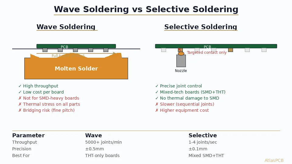
Wave Soldering: Process Fundamentals
How Wave Soldering Works
Wave soldering exposes the entire bottom surface of a PCB to a controlled wave of molten solder:
- Flux application: Spray flux coats the board bottom (foam, spray, or wave fluxing)
- Preheating: IR or convection heaters raise the board to 100-130°C (reducing thermal shock)
- Wave contact: The board passes over a standing solder wave at 245-265°C
- Separation: Board exits the wave; surface tension and drainage remove excess solder
- Cooling: Forced-air or natural cooling solidifies joints
The entire process takes 3-5 minutes per board, but since boards run continuously on a conveyor, effective throughput reaches 60-120 boards per hour depending on board length and conveyor speed.
Wave Types
Modern wave soldering machines use dual-wave configurations:
Chip wave (turbulent/lambda wave):
- Turbulent, high-velocity solder flow
- Penetrates tight spaces between leads
- Eliminates shadowing behind large components
- Critical for bottom-side SMD components (when palletized)
Laminar wave (smooth wave):
- Smooth, controlled solder surface
- Clean peel-off reducing bridges and icicles
- Sets final fillet geometry
- Follows chip wave in sequence
Wave Soldering Advantages
- Throughput: 5,000+ joints per minute (all joints simultaneously)
- Cost per joint: $0.02-0.05 at volume (>10,000 boards)
- Consistency: Every board sees identical thermal profile
- Mature process: 50+ years of industry optimization
- Nitrogen-compatible: Inert atmosphere option reduces dross
Wave Soldering Limitations
- Full-board thermal exposure: Bottom-side SMD components see wave temperatures
- Palletizing required: Mixed-tech boards need custom carriers ($3,000-8,000 per design)
- Bridging risk: Fine-pitch components (≤1.27mm) prone to solder bridges
- Dross generation: Lead-free operation generates significant oxidation waste
- Thermal stress: Entire board experiences ΔT >200°C
Selective Soldering: Process Fundamentals
How Selective Soldering Works
Selective soldering applies solder only to designated through-hole joints using programmable nozzles:
- Flux dispensing: Precision drop-jet or spray applies flux only to target joints
- Preheating: Bottom-side IR preheats localized areas to 80-110°C
- Soldering: A small nozzle (2-12mm diameter) rises to contact specific pads
- Dwell & withdrawal: Nozzle holds contact (2-5 seconds per joint), then retracts
- Indexing: Machine moves to next programmed solder point
Selective Soldering Methods
Single-point nozzle:
- 2-6mm nozzle for individual joints
- Maximum flexibility and precision
- Typical speed: 1-2 joints per second
- Best for complex, low-quantity boards
Multi-point nozzle (mini-wave):
- 8-60mm custom nozzle matching connector footprint
- Solders entire connector in one pass
- Speed: one connector per 3-5 seconds
- Requires nozzle tooling per footprint
Dip soldering (selective variant):
- Board dips specific areas into small solder pot
- Middle ground between wave and point-selective
- Suitable for consistent through-hole clusters
Selective Soldering Advantages
- Mixed-technology compatible: No thermal damage to bottom-side SMDs
- No palletizing: Eliminates fixture cost and lead time
- Fine-pitch capable: Programmable parameters per joint prevent bridging
- Process flexibility: Different flux, temperature, dwell per joint group
- Lower defect rate: 50-200 PPM vs. 500-2000 PPM for wave (mixed-tech)
Selective Soldering Limitations
- Sequential processing: 1-4 joints per second (vs. 5,000+ for wave)
- Higher per-joint cost: $0.05-0.15 per joint at volume
- Equipment cost: $150K-500K for advanced selective machines
- Programming time: Initial setup requires 2-8 hours per new product
- Nozzle maintenance: Wetting degradation requires periodic replacement
🔧 Need PCB Assembly with Optimal Soldering Process?
AtlasPCB provides full turnkey assembly with both wave and selective soldering capabilities. Our engineers recommend the optimal process for your board's technology mix. DFM review included with every order.
Get Your Free DFM Review →Head-to-Head Comparison
| Parameter | Wave Soldering | Selective Soldering |
|---|---|---|
| Speed | 5,000+ joints/min | 1-4 joints/sec |
| Cost per joint | $0.02-0.05 | $0.05-0.15 |
| Positioning accuracy | ±0.5mm (board-level) | ±0.1mm (joint-level) |
| Temperature control | Global (entire board) | Per-joint programmable |
| Mixed-tech capability | Requires palletizing | Native support |
| Fine-pitch (≤1.27mm) | High bridge risk | Controllable |
| Lead-free dross | 30-50% by weight | <5% (enclosed nozzle) |
| Setup cost | Pallet: $3K-8K | Programming: $500-1K |
| Volume sweet spot | >10,000 boards/run | 100-5,000 boards/run |
| Defect rate (mixed-tech) | 500-2000 PPM | 50-200 PPM |
Defect Profiles: Wave vs. Selective
Common Wave Soldering Defects
Bridging: Solder connects adjacent pins (especially fine-pitch)
- Cause: Insufficient drainage between pins
- Mitigation: Thief pads, nitrogen, reduced contact time
Icicles/spikes: Pointed solder protrusions
- Cause: Oxidized wave surface, insufficient peel-off
- Mitigation: Nitrogen blanket, optimize wave height
Skip/insufficient: Missing or thin solder fillets
- Cause: Contaminated pads, shadowing by large components
- Mitigation: Dual-wave configuration, adjust board angle
Blow holes: Gas voids in solder barrel
- Cause: Moisture in PCB expands during wave contact
- Mitigation: Pre-bake boards, extend preheat
Common Selective Soldering Defects
Cold joints: Dull, grainy fillet appearance
- Cause: Insufficient dwell time or temperature
- Mitigation: Increase contact time, verify nozzle wetting
Insufficient fill: Barrel not fully wetted
- Cause: Inadequate flux activation, nozzle too small
- Mitigation: Adjust flux volume, increase preheat temperature
Flux residue: Excessive flux around joints
- Cause: Over-dispensing or incomplete thermal activation
- Mitigation: Calibrate dispenser volume, adjust preheat profile
Design for Soldering (DFS) Guidelines
Designing for Wave Soldering
When your design will use wave soldering, follow these PCB layout rules:
- Orientation: Orient elongated components (SIPs, connectors) perpendicular to wave direction
- Spacing: Minimum 1.5mm between adjacent THT pads on wave side
- Thief pads: Add sacrificial pads downstream of fine-pitch components
- Thermal relief: Use full thermal connections (no thermals) for better wave fill
- [Solder mask]/blog/pcb-solder-mask-types-application-dfm/): Ensure mask dams between pads ≥0.1mm
Designing for Selective Soldering
For selective soldering optimization:
- Keep-out zones: Maintain 5mm clearance around target joints (for nozzle access)
- Board flatness: Specify ≤0.5mm warp in selective solder area
- Component height: Bottom-side components ≤3mm in selective zone
- Pad accessibility: No overhanging components blocking nozzle approach
- Fiducials: Add 2-3 fiducials for machine vision alignment
Mixed-Technology Layout Strategies
For boards requiring both SMD and through-hole components:
- Group THT components: Cluster through-hole parts to minimize selective solder moves
- Separate thermal zones: Keep large thermal-mass THT parts away from sensitive SMDs
- Panel orientation: Consider selective solder nozzle travel when designing panel layout
- DFM review: Have your assembler review the layout before finalizing
Cost Analysis: When to Choose Each Process
Wave Soldering is More Economical When:
- Board has >50 through-hole joints
- No bottom-side SMD components (or all-THT design)
- Production volume exceeds 10,000 boards per run
- Component pitch is ≥2.54mm throughout
- Board design is stable (amortizes pallet cost)
Selective Soldering is More Economical When:
- Board has <30 through-hole joints on a mixed-tech board
- Bottom-side SMD components present (palletizing eliminated)
- Production volume is 100-5,000 boards per run
- Multiple product variants share the same line
- Fine-pitch connectors require joint-by-joint control
Break-Even Analysis
For a typical mixed-technology board with 20 THT joints:
Wave soldering total cost:
  Pallet tooling: $5,000 (amortized over run)
  Per-board wave: $1.50
  Manual touch-up: $2.00 (for bridging fixes)
  Total at 1,000 units: $5,000 + (1,000 × $3.50) = $8,500

Selective soldering total cost:
  Programming setup: $800
  Per-board selective: $3.00
  Touch-up (minimal): $0.25
  Total at 1,000 units: $800 + (1,000 × $3.25) = $4,050
At 1,000 units, selective soldering saves 52%. The break-even point shifts to wave soldering around 5,000-8,000 units depending on board complexity.
Lead-Free Considerations
Both processes support lead-free soldering (SAC305, SAC0307, SN100C), but with different challenges:
Lead-Free Wave Soldering
- Pot temperature: 255-265°C (vs. 245-250°C SnPb)
- Dross rate: 30-50% higher than leaded
- Copper dissolution: 0.8-1.2 μm/sec (vs. 0.3-0.5 leaded)
- Nitrogen mandatory for acceptable dross levels
- Nozzle/pump materials: Titanium or ceramic-coated (resist erosion)
Lead-Free Selective Soldering
- Nozzle temperature: 260-280°C
- Enclosed nozzle design minimizes oxidation
- Lower solder consumption (targeted application)
- Longer dwell times required (3-5 sec vs. 2-3 sec leaded)
- Less copper dissolution risk (shorter contact per joint)
Process Selection Flowchart
Start: Does your board have bottom-side SMDs?
├── YES → Selective soldering (or palletized wave if >10K volume)
└── NO → Is all pitch ≥2.54mm?
    ├── YES → Wave soldering (most economical)
    └── NO → Fine-pitch joints?
        ├── <20 fine-pitch joints → Selective for fine-pitch, wave for rest
        └── >20 fine-pitch joints → Full selective soldering
Integration with [Reflow Soldering]/blog/reflow-soldering-profile-optimization-lead-free-pcb-assembly/)
Modern assembly lines typically process boards in this sequence:
- Solder paste print → SMD placement → Reflow (top and bottom SMDs)
- Through-hole insertion (manual or auto-insertion)
- Wave OR selective soldering (THT joints only)
- [Inspection]/blog/aoi-spi-inspection-pcb-assembly-quality-control/) (AOI + X-ray for BGA if present)
The choice between wave and selective in step 3 depends on the factors discussed above.
Conclusion
Wave soldering remains the throughput champion for high-volume, THT-dominant assemblies. Selective soldering wins for mixed-technology boards, low-to-medium volumes, and designs requiring fine-pitch precision without the cost and lead time of custom pallets.
For most modern designs—which combine SMD and THT—selective soldering has become the default recommendation unless volumes clearly justify wave soldering infrastructure.
Further Reading
- [PCBA Assembly Process Guide]/blog/pcba-assembly-process/) — Complete assembly flow overview
- [Reflow Soldering Profile Optimization]/blog/reflow-soldering-profile-optimization-lead-free-pcb-assembly/) — Lead-free reflow engineering
- [SMT vs Through-Hole Assembly]/blog/smt-vs-through-hole-assembly/) — Technology comparison
- [AOI & SPI Inspection]/blog/aoi-spi-inspection-pcb-assembly-quality-control/) — Post-solder quality verification
About AtlasPCB — We specialize in complex PCB manufacturing for HDI, RF, and high-reliability applications. Explore our PCB assembly services . Every order includes free engineering review. Get your quote.
Reviewed by AtlasPCB Engineering Team — IPC-certified manufacturing specialists with 15+ years of production experience in HDI, RF, and high-reliability PCB fabrication. Content based on factory floor data and real customer design reviews.
- wave-soldering
- selective-soldering
- pcb-assembly
- through-hole
- manufacturing-process